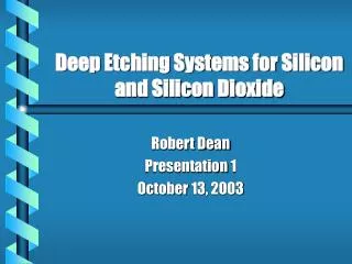
Deep Etching Systems for Silicon and Silicon Dioxide
540 likes | 1.94k Vues
Deep Etching Systems for Silicon and Silicon Dioxide. Robert Dean Presentation 1 October 13, 2003. Questions. How does the Bosch process reduce sidewall etching? In the AOE process, what effect does increasing the H 2 concentration have on the etch rate?. Introduction. Terminology

Deep Etching Systems for Silicon and Silicon Dioxide
E N D
Presentation Transcript
Deep Etching Systems for Silicon and Silicon Dioxide Robert Dean Presentation 1 October 13, 2003
Questions • How does the Bosch process reduce sidewall etching? • In the AOE process, what effect does increasing the H2 concentration have on the etch rate?
Introduction • Terminology • SOI wafers for MEMS fabrication • The Bosch process • ICP etchers • The STS ASE Bosch process • The STS AOE Process
Why Deep Etching? • Fabrication of MEMS (microelectro-mechanical systems) devices • Fabrication of micro optical devices • Fabrication of cavities and structures for specialty packaging • Fabrication of micro tooling, such as shadow masks
Etching Terminology • Mask • A layer, usually temporary, that protects a material underneath during an etching process • Isotropic Etch • An etching process that etches at the same rate in all directions • Anisotropic Etch • An etching process that etches at different rates in different directions • Aspect Ratio • The ratio of depth to width of an etched feature: a metric for evaluating an etch • Undercutting • The often undesirable result of an etching process where material is removed from up under a mask or other layer. Robert Dean (invited speaker), “An Introduction to MEMS,” a three-hour short course, Center for Advanced Vehicle Electronics semiannual meeting, Auburn University, April 17, 2002.
Isotropic Etch Etch Mask Anisotropic Etch Undercutting Etching Target Etching Terminology Illustration Robert Dean (invited speaker), “An Introduction to MEMS,” a three-hour short course, Center for Advanced Vehicle Electronics semiannual meeting, Auburn University, April 17, 2002.
SOI Wafers • SOI: “Silicon on Insulator” • A silicon wafer comprised of 3 sections: • Top or “device” layer: a thin silicon layer • Middle or “box” layer: a thin layer of silicon dioxide • Bottom or “handle” layer: a thick silicon layer • Useful for MEMS and advanced microelectronics • Several methods for fabricating SOI wafers Richard W. Lusignea, “Liquid Crystal Polymers: New Barrier Materials for Packaging”, Packaging Technology, October 1997.
Device Layer: 2m to 100m thick Box Layer: 0.5m to 5m thick Handle layer: 300m to 725m thick Silicon Device Layer SiO2 Box Layer Silicon Handle Typical SOI Wafer Characteristics http://www.ultrasil.com/quote.html
An SOI Wafer Fabrication Process: Wafer Bonding • Start with 2 Si wafers • Grow or deposit SiO2 on the polished side(s) of one or both wafers • Wafer bond the 2 wafers together at the SiO2 interface • Chemical-mechanical polish (CMP) one of the wafers down to the desired Device layer thickness http://www.isonics.com/frameset.cfm?dir=products/SOIwafers
Desirability of SOI for MEMS • Si devices of a desired thickness are attached to a Si frame (same CTE and other properties) • Simplified microfabrication: • 1 photolithography mask • 1 or 2 dry etches • dice • HF oxide release etch • E-beam metallization
Example SOI Based MEMS Device MEMS Gyroscope Chip Courtesy Morgan Research Corporation
Limitations of Standard RIE • RIE Process: • Energetic ions bombard the surface at 90o • Reactive neutrals etch all exposed surfaces • Aspect ratio is limited to about 15 • For a 100m deep etch: 6.7m horizontal etch at the top of the trench • Unacceptable for many MEMS applications T. Shu, “MEMS & Microsystems Design and Manufacture”, McGraw-hill, New York, pp.315-318, 2002.
Illustration of a Shallow RIE Etch T. Shu, “MEMS & Microsystems Design and Manufacture”, McGraw-hill, New York, pp.315-318, 2002.
Illustration of a “Deep” RIE Etch Tapered sidewalls Deep RIE is called DRIE T. Shu, “MEMS & Microsystems Design and Manufacture”, McGraw-hill, New York, pp.315-318, 2002.
The Bosch Process • Patented modified RIE process that yields a higher aspect ratio than standard RIE • Sequential alternating process of etching and passivation • Aspect ratios of 20 or higher F. Laermer and A. Schilp, Method of Anisotropically Etching Silicon, US Patent Number: 5501893, 1996. AND S. A McAuley. H. Ashraf, L. Atabo, A. Chambers, S. Hall, J. Hopkins and G. Nicholls, "Silicon Micromachining Using a High-density Plasma Source", Journal of Physics D: Applied Physics, Vol. 34, pp. 2769-2774, 2001
Etching System Characteristics • High pressure plasma (100 to 500mtorr) • 2.45GHz microwave plasma generation • 13.56MHz RF source used to bias the Si substrate at -5 to -30V • Gas chemistry: C4F8, SF6 and Ar • He backcooling used to keep the Si substrate at the optimum temperature F. Laermer and A. Schilp, Method of Anisotropically Etching Silicon, US Patent Number: 5501893, 1996. AND S. A McAuley. H. Ashraf, L. Atabo, A. Chambers, S. Hall, J. Hopkins and G. Nicholls, "Silicon Micromachining Using a High-density Plasma Source", Journal of Physics D: Applied Physics, Vol. 34, pp. 2769-2774, 2001
Sequential Alternating Process of Etching and Passivation • Etching: • SF6/Ar plasma RIE etch • Positive ions bombard substrate at ~90o, sputtering horz. surfaces • Passivation: • C4F8 and SF6 chemically combine to form polymerized CF2 • Deposits a Teflon like polymer layer on all surfaces • Next etching step • 90o bombarding ions etch through the coating on horizontal surfaces and continue sputtering the Si • Polymer layer protects vertical surfaces from reactive neutrals F. Laermer and A. Schilp, Method of Anisotropically Etching Silicon, US Patent Number: 5501893, 1996. AND S. A McAuley. H. Ashraf, L. Atabo, A. Chambers, S. Hall, J. Hopkins and G. Nicholls, "Silicon Micromachining Using a High-density Plasma Source", Journal of Physics D: Applied Physics, Vol. 34, pp. 2769-2774, 2001
Illustration of the Bosch Process Sidewall passivation layer T. Shu, “MEMS & Microsystems Design and Manufacture”, McGraw-hill, New York, pp.315-318, 2002.
Limitations of the Bosch Process • Does not work for DRIE on SOI wafers • As the device layer etch approaches the SiO2 layer, positive charge accumulates on the insulating SiO2 layer • This deflects the incident positive ions into the sidewalls • Results in severe undercutting in the Si sidewalls at the bottom of the trench C. Gormley, K. Yallup, W. A. Nelvin; BCO Technologies; J. Bhardwaj and H. Ashraf, Surface Technology Systems Ltd.; P. Huggett, Orbis Technologies; and S. blackstone, BCO America, “State of the Art Deep Silicon Anisotropic Etching on SOI bonded Substrates for Dielectric Isolation and MEMS Applications”, Fifth International Symposium on Semiconductor Wafer Bonding: Science, Technology and Applications, The Fall Meeting of the Electrochemical Society, Hawaii, October 17-22, 1999.
Inductively Coupled Plasma (ICP) Systems • RF power (13.56MHz typically) is coupled into the plasma through transformer action • Common system configuration: • quartz tube containing the low pressure gas • wrapped with 2 to 8 turns of cable • Able to achieve high density plasmas at low pressure (<10mtorr) • Separate RF supply for substrate biasing S. A McAuley. H. Ashraf, L. Atabo, A. Chambers, S. Hall, J. Hopkins and G. Nicholls, "Silicon Micromachining Using a High-density Plasma Source", Journal of Physics D: Applied Physics, Vol. 34, pp. 2769-2774, 2001. AND J. R. Roth, "Industrial Plasma Engineering, Volume 1", Institute of Physics Publishing Ltd., Philadelphia, pp. 392-393, 1995.
Drawing of an Example ICP Configuration J. R. Roth, "Industrial Plasma Engineering, Volume 1", Institute of Physics Publishing Ltd., Philadelphia, pp. 392-393, 1995.
Advantages of ICP Etching Systems • High density plasmas have higher etch rates than low density plasmas • Maintain a high coupling efficiency between the applied RF electric field and the electrons in the plasma • Solenoidal magnetic field: • Improves plasma confinement • Reduces electron loss from wall collisions S. A McAuley. H. Ashraf, L. Atabo, A. Chambers, S. Hall, J. Hopkins and G. Nicholls, "Silicon Micromachining Using a High-density Plasma Source", Journal of Physics D: Applied Physics, Vol. 34, pp. 2769-2774, 2001. AND J. R. Roth, "Industrial Plasma Engineering, Volume 1", Institute of Physics Publishing Ltd., Philadelphia, pp. 392-393, 1995.
Advantages of ICP Etching Systems, Continued • Reduced ion scattering from fewer collisions in the low pressure system • Improved transport of etch species into deeply etched trenches • Reduced mask erosion and substrate damage when increasing the etchant species S. A McAuley. H. Ashraf, L. Atabo, A. Chambers, S. Hall, J. Hopkins and G. Nicholls, "Silicon Micromachining Using a High-density Plasma Source", Journal of Physics D: Applied Physics, Vol. 34, pp. 2769-2774, 2001. AND J. R. Roth, "Industrial Plasma Engineering, Volume 1", Institute of Physics Publishing Ltd., Philadelphia, pp. 392-393, 1995.
The ASE Bosch Process • ASE: “advanced silicon etch ” • Integration of the Bosch process into an ICP etching system • Surface Technology Systems, Ltd. (STS) produces these systems ] C. Gormley, K. Yallup, W. A. Nelvin; BCO Technologies; J. Bhardwaj and H. Ashraf, Surface Technology Systems Ltd.; P. Huggett, Orbis Technologies; and S. blackstone, BCO America, “State of the Art Deep Silicon Anisotropic Etching on SOI bonded Substrates for Dielectric Isolation and MEMS Applications”, Fifth International Symposium on Semiconductor Wafer Bonding: Science, Technology and Applications, The Fall Meeting of the Electrochemical Society, Hawaii, October 17-22, 1999.
System Characteristics • 1kW, 13.56MHz RF source used to generate the plasma • A variable frequency RF source used to bias the substrate • The substrate is electrostatically clamped to the platen • Helium backcooling used to keep the substrate at 80oC • Optical emission spectroscopy (OES) used for endpoint detection • Operated under software control ] C. Gormley, K. Yallup, W. A. Nelvin; BCO Technologies; J. Bhardwaj and H. Ashraf, Surface Technology Systems Ltd.; P. Huggett, Orbis Technologies; and S. blackstone, BCO America, “State of the Art Deep Silicon Anisotropic Etching on SOI bonded Substrates for Dielectric Isolation and MEMS Applications”, Fifth International Symposium on Semiconductor Wafer Bonding: Science, Technology and Applications, The Fall Meeting of the Electrochemical Society, Hawaii, October 17-22, 1999.
Drawing of an STS ASE Bosch Process Etcher J. Bhardwaj, H. Ashraf, A. McQuarrie, “Dry Silicon Etching for MEMS”, The Symposium on Microstructures and Microfabricated Systems, The Annual Meeting of the Electrochemical Society, Montreal, Quebec, Canada. May 4-9, 1997.
Photograph of STS ASE Bosch Process Etcher Courtesy Auburn University microfabrication laboratory
Typical Process Characteristics • For etching 100mm and 150mm diameter silicon wafers: • Etch Rate: 1.5 to 3.0m/min • Aspect Ratio: Up to 30 • Selectivity to SiO2: 120 to 200:1 • Selectivity to PR: 50 to 100:1 • Sidewall Profile: 90o2o • Feature Size: 1 to >500m • Etch Depth Capability: 10 to 800m J. Bhardwaj, H. Ashraf, A. McQuarrie, “Dry Silicon Etching for MEMS”, The Symposium on Microstructures and Microfabricated Systems, The Annual Meeting of the Electrochemical Society, Montreal, Quebec, Canada. May 4-9, 1997.
Parameter Ramping • The etch process is optimized throughout the etch by ramping the RF power - “parameter ramping” • Beginning of the etch: low power • low mask sputtering • low Si etch rate • End of the etch: high power • higher mask sputtering • higher Si etch rate • facilitates passivation removal at the trench bottom • better transport of etch species to bottom of deep trenches • Results in good overall process characteristics S. A McAuley. H. Ashraf, L. Atabo, A. Chambers, S. Hall, J. Hopkins and G. Nicholls, "Silicon Micromachining Using a High-density Plasma Source", Journal of Physics D: Applied Physics, Vol. 34, pp. 2769-2774, 2001.
Applicable to Etching SOI Wafers • When approaching the SiO2 layer, the frequency of the platen RF supply is lowered from 13.56MHz to 380KHz • The positive ions can respond to the lower frequency • Results in more low energy ions possessing low directionality • These ions neutralize negative charge accumulating at the top of the trench • This allows electrons to reach the bottom of the trench and neutralize the positive charge • Greatly reduces trench-bottom sidewall undercutting ] C. Gormley, K. Yallup, W. A. Nelvin; BCO Technologies; J. Bhardwaj and H. Ashraf, Surface Technology Systems Ltd.; P. Huggett, Orbis Technologies; and S. blackstone, BCO America, “State of the Art Deep Silicon Anisotropic Etching on SOI bonded Substrates for Dielectric Isolation and MEMS Applications”, Fifth International Symposium on Semiconductor Wafer Bonding: Science, Technology and Applications, The Fall Meeting of the Electrochemical Society, Hawaii, October 17-22, 1999.
Photograph of an SOI wafer Etched to the Buried Oxide Little Undercutting ] C. Gormley, K. Yallup, W. A. Nelvin; BCO Technologies; J. Bhardwaj and H. Ashraf, Surface Technology Systems Ltd.; P. Huggett, Orbis Technologies; and S. blackstone, BCO America, “State of the Art Deep Silicon Anisotropic Etching on SOI bonded Substrates for Dielectric Isolation and MEMS Applications”, Fifth International Symposium on Semiconductor Wafer Bonding: Science, Technology and Applications, The Fall Meeting of the Electrochemical Society, Hawaii, October 17-22, 1999.
MEMS fuel atomizer SOI implementation Fabricated using the ASE Bosch process 2 DRIE etches: From the front side From the back side Example MEMS Device 1 J. Bhardwaj, H. Ashraf, A. McQuarrie, “Dry Silicon Etching for MEMS”, The Symposium on Microstructures and Microfabricated Systems, The Annual Meeting of the Electrochemical Society, Montreal, Quebec, Canada. May 4-9, 1997.
MOEMS fiber optic switch SOI implementation Fabricated using the ASE Bosch process Single DRIE etch Electrostatic actuator positions mirror Example MEMS Device 2 S. A McAuley. H. Ashraf, L. Atabo, A. Chambers, S. Hall, J. Hopkins and G. Nicholls, "Silicon Micromachining Using a High-density Plasma Source", Journal of Physics D: Applied Physics, Vol. 34, pp. 2769-2774, 2001.
The AOE Process • AOE: “advanced oxide etch ” • Consists of a non-Bosch process ICP etching system • Surface Technology Systems, Ltd. (STS) produces these systems • Used to perform deep etches in silicon dioxide wafers • Applications include MEMS, micro-optics, packaging J. Bhardwaj, H. Ashraf, J. Hopkins, I, Johnston, S. McAuley, S. Hall, G. Nicholls, L. Atabo, A. Hynes, C. Welch, A. Barker, B. Gunn, L. Lea, E. Guibarra, and S. Watcham, “Advances in High Rate Silicon and Oxide Etching using ICP”, MEMS/MST Technology Symposium at SEMICON West 99, San Francisco, CA, July 12-16, 1999.
System Characteristics • 1kW, 13.56MHz RF source used to generate the plasma • Multipolar magnetic plasma confinement utilized • Typical chamber pressure of 3mtorr • 300W, 13.56Mhz RF source used to bias the substrate • Wafer electrode temperature typically 10oC • Gas Chemistry utilized: C4F8/Ar/H2 • System is operated under software control J. Bhardwaj, H. Ashraf, J. Hopkins, I, Johnston, S. McAuley, S. Hall, G. Nicholls, L. Atabo, A. Hynes, C. Welch, A. Barker, B. Gunn, L. Lea, E. Guibarra, and S. Watcham, “Advances in High Rate Silicon and Oxide Etching using ICP”, MEMS/MST Technology Symposium at SEMICON West 99, San Francisco, CA, July 12-16, 1999.
Additional System Characteristics • Aluminum plasma chamber (magnetic confinement • Recirculating DI water system and a helium backcooling system used to control temperature of the wafer platen and coil • Chamber Heaters used to heat the plasma in some applications • Sofie Digitwin end point detection system (optical emission spectroscopy and reflectance interferometry “Mesc Multiplex AOE Operator’s Manual”, Surface Technology Systems Limited, UK, December 1999, pp. 1-5, 1-18, and 2-9 .
Drawing of an STS AOE Etcher J. Bhardwaj, H. Ashraf, J. Hopkins, I, Johnston, S. McAuley, S. Hall, G. Nicholls, L. Atabo, A. Hynes, C. Welch, A. Barker, B. Gunn, L. Lea, E. Guibarra, and S. Watcham, “Advances in High Rate Silicon and Oxide Etching using ICP”, MEMS/MST Technology Symposium at SEMICON West 99, San Francisco, CA, July 12-16, 1999.
Typical Process Characteristics • Etch Rate: 0.4 to 0.5m/min • Typical masks: Poly Si, PR, Ni • Selectivity to poly Si: 25:1 • Sidewall Profile: >89o • Etch uniformity: within 2% • Etch Depth Capability: at least 100m J. Bhardwaj, H. Ashraf, J. Hopkins, I, Johnston, S. McAuley, S. Hall, G. Nicholls, L. Atabo, A. Hynes, C. Welch, A. Barker, B. Gunn, L. Lea, E. Guibarra, and S. Watcham, “Advances in High Rate Silicon and Oxide Etching using ICP”, MEMS/MST Technology Symposium at SEMICON West 99, San Francisco, CA, July 12-16, 1999.
Gas Ratio Adjustments and Process Control Etch rate of oxide as a function of H2 addition to C4F8/Ar Selectivity of PR and poly Si as a function of H2 addition to C4F8/Ar J. Bhardwaj, H. Ashraf, J. Hopkins, I, Johnston, S. McAuley, S. Hall, G. Nicholls, L. Atabo, A. Hynes, C. Welch, A. Barker, B. Gunn, L. Lea, E. Guibarra, and S. Watcham, “Advances in High Rate Silicon and Oxide Etching using ICP”, MEMS/MST Technology Symposium at SEMICON West 99, San Francisco, CA, July 12-16, 1999.
40m Etch in Deep PECVD Oxide J. Bhardwaj, H. Ashraf, J. Hopkins, I, Johnston, S. McAuley, S. Hall, G. Nicholls, L. Atabo, A. Hynes, C. Welch, A. Barker, B. Gunn, L. Lea, E. Guibarra, and S. Watcham, “Advances in High Rate Silicon and Oxide Etching using ICP”, MEMS/MST Technology Symposium at SEMICON West 99, San Francisco, CA, July 12-16, 1999.
95m Deep Etch in Quartz Nickel Mask Quartz Substrate J. Bhardwaj, H. Ashraf, J. Hopkins, I, Johnston, S. McAuley, S. Hall, G. Nicholls, L. Atabo, A. Hynes, C. Welch, A. Barker, B. Gunn, L. Lea, E. Guibarra, and S. Watcham, “Advances in High Rate Silicon and Oxide Etching using ICP”, MEMS/MST Technology Symposium at SEMICON West 99, San Francisco, CA, July 12-16, 1999.
Conclusions • SOI wafers are particularly useful for MEMS devices • Conventional RIE and the Bosch process are not appropriate for fabricating MEMS devices in SOI wafers • The ASE Bosch process is appropriate for fabricating MEMS devices in SOI wafers. • The AOE process is useful for deep etching of silicon dioxide wafers
Answers to Questions • The Bosch process reduces sidewall etching by using a sequential alternating process of etching and passivation to reduce isotropic etching by reactive neutrals on the sidewalls. • Increasing the H2 concentration reduces the etch rate.