Workshop Testing Results for Silicon Sensors at Purdue University
Analysis of I-V characteristics and various parameters of silicon sensors tested at Purdue University's workshop. Results including depletion voltage, capacitance, leakage current, and sensor performance under different conditions are detailed.

Workshop Testing Results for Silicon Sensors at Purdue University
E N D
Presentation Transcript
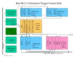
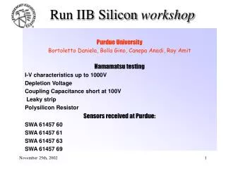
Run IIB Silicon workshop Purdue University Bortoletto Daniela, Bolla Gino, Canepa Anadi, Roy Amit Hamamatsu testing I-V characteristics up to 1000V Depletion Voltage Coupling Capacitance short at 100V Leaky strip Polysilicon Resistor Sensors received at Purdue: SWA 61457 60 SWA 61457 61 SWA 61457 63 SWA 61457 69
Run IIB Silicon workshop Purdue Testing results at www.physics.purdue.edu/cdf/RunIIB/pres sensor characterization I-V characteristics up to 1000V Depletion Voltage Coupling Capacitance & Oxide Leakage Current Polysilicon Resistor Interstrip Capacitance Radiation Hardness Test sensor SWA61457 60 sensor SWA61457 63 sensor SWA61457 69 have been irradiated at U.C.Davies facility fluence = 1.4 1014 1MeV eq-n cm-2 fully characterizated
Run IIB Siliconworkshop Sensor 60 I (120V) =62.6nA hamamatsu I(120V)=77.3nA Sensor 61 (bonding problems) I (V=150) =120nA hamamatsu I(150)=71 nA Sensor 63 I (V=140)=71nA hamamatsu I(140)=74.3nA Sensor 69 I (140V) =76.8nA hamamatsu I(140V)=81.3nA
Run IIB Siliconworkshop Neutron irradiation fluence 1.4 1014 1MeV n-eq cm^-2 Layer 0 Operating temperature T = -5C (TDR 3-16) Leakage current per strip module Istrip(V > Vd) 95 nA
Run IIB Siliconworkshop Annealing procedure on sensor 69 4min @ T=80C Both sensor 60 and sensor 69 I(plateau) 50uA (T = -25C) sensor 60:1400 min at T=20C sensor 69: 800 min at T = 20C & annealing Before Irradiation breakdown voltage =181V Assuming a=410-17 A/cm DI(Vdep) 7mA Measured value DI(Vdep) 5.5mA Estimated Fluence = 1.1 1014 1MeV n-eq
Run IIB Siliconworkshop Sensor 60 Vdep=117 V hamamatsu Vdep=140V Sensor 61 Vdep=141 V hamamatsu Vdep=160V Sensor 63 Vdep=133 V hamamatsu Vdep=160V Sensor 69 Vdep=132 V hamamatsu Vdep=150V
Run IIB Siliconworkshop ROSE/TN/2000-10 Version 1/14.12/2000 Vd (20C)=Vd(T)*1.0526/[1+A·exp(T/t)] A=0.00936 t = 11.58 Vd(f)=Vd(1kHz)[1-D·log(f/1kHz)] D=0.11+/-0.009 After irradiation Sensor 60 T=-25C,f=1kHz Vdep=137 V T=20C,f=10kHz Vdep=128 V
Run IIB Siliconworkshop After irradiation Sensor 69 Vdep(T=20C,f=100kHz) =136 V Vdep(T=20C,f=10kHz) =119 V After irradiation & after annealing Sensor 69 to be understood
Run IIB Siliconworkshop Open in the metal ? Sensor 60 Coupling Capacitance CC(100Hz)= 134.43+/-0.48pF Sensor 63 Coupling Capacitance CC(100Hz)= 125.32+/-1.99pF Sensor 690 Coupling Capacitance CC(100Hz)= 126.49+/-0.97pF
Run IIB Siliconworkshop Sensor 60 Coupling Capacitance CC(100Hz)= 136.34+/-1.17pF Sensor 69 Coupling Capacitance CC(100Hz)= 134.47+/-5.34pF
Run IIB Siliconworkshop Trend to be understood ? Sensor 60 Interstrip Capacitance Ci(1MHz)= 3.46+/-1.68pF Sensor 63 Interstrip Capacitance Ci(1MHz)= 3.17+/-0.01pF Sensor 69 Interstrip Capacitance Ci(1MHz)= 3.53+/-0.18pF
Run IIB Siliconworkshop Sensor 63 Interstrip Capacitance Ci(1MHz)= 3.39+/-0.07pF Sensor 60 Interstrip Capacitance Ci(1MHz)= 3.43+/-0.08pF
Run IIB Siliconworkshop Before Irradiation Sensor 60 R=1.72 +/- 0.2 MOhm Sensor 63 R=1.84 +/- 0.8 Mohm drop to be understood charge up ? After Irradiation Sensor 63 R=1.64 +/- 0.04 MOhm Sensor 63 R=1.7 +/- 0.8 Mohm
Run IIB Siliconworkshop Before Irradiation R=1.86 MOhm After Irradiation R=1.71 MOhm
Run IIB Siliconworkshop Conclusions We have evaluated the performance of Axial Outer Layer The sensors fulfill the specifications: Leakage Current as Small as expected Bad channel Not found Capacitance Values as Expected Bias Resistor as Expected Full Dep Voltage after Irradiation as Expected NEED to be understood: 1)Before Irradiation, Bias Resistance drop : Charge up ? 2)After Irradiation, Interstrip Capacitance bump : related to Bias Resistor ? 3)After Irradiation & After annealing, Total Capacitance increase at V>Vdep