CDF Run II Silicon
170 likes | 410 Vues
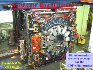
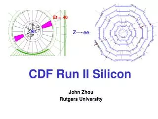
CDF Run II Silicon. Z ee. John Zhou Rutgers University. Run II!. CDF Silicon Run II Motivation: tracking b quarks for top Higgs CP Violation Exotics Run II as of end of October Large fraction of data were taken with silicon

CDF Run II Silicon
E N D
Presentation Transcript
CDF Run II Silicon Z ee John Zhou Rutgers University
Run II! • CDF Silicon Run II Motivation: tracking b quarks for • top • Higgs • CP Violation • Exotics • Run II as of end of October • Large fraction of data were taken with silicon • Achieving higher silicon inclusion efficiency month by month
Silicon Overview • 8 Layers, 704 ladders, 722432 Chans • Layer 00 (L00): 1 Single Sided layer • SVXII: 5 Double Sided Layers • ISL: 2 Double Sided Layers • One of largest and most complex silicon system ever built SVX-3 Chip
SVXII Barrels • 5 DS Layers (3 90o, 2 1.2o), 2.5 < r < 10.6 cm, l = 0.9 m, greatly enhanced coverage • 360 ladders, 405504 Chan. • Standalone 3D tracking • “Displaced track” trigger
Intermediate Silicon Layers (ISL) • Linking COT to the SVX for optimal tracking performance • Extends tracking to ||=2 • 2 DS 1.2o layers, r = 20,28 cm, l = 1.9 m! • 296 ladders, 303104 Chans 1 m 1 meter The ISL doubles the pseudorapidity range for b tagging and lepton id.
Layer 00: Beampipe Layer • SS layer on beampipe • 48 ladders, 13824 Chans • Increases IP (Impact Parameter) resolution by factor of 2 at pT = 1 GeV/c cables SVX inner bore silicon Be beam pipe 2.2 cm Cooling tube channel C fiber support
NSF at More Silicon Projects Power Supply (Johns Hopkins) Secondary Vertex Trigger (Chicago) SVT Board (Chicago) Cables (Johns Hopkins)
NSF at Silicon Vertex Detector • Sensor Testing • Beam Testing • Production Testing • Burn-in • Calibration • Alignment • Monitoring Si Ladder inspection (Rutgers) Si Burn-in Box (Rutgers) Si Burn-in System (Rutgers) SVT Board (UC)
Jumper HV Problem Fixed • Jumper did not hold high voltage • Takes signal, HV from phi side to z side • Signal/ground traces close to HV traces • Found after ~20 hours of Burn-In crucial test • Solution: Copper wire for HV traces Bus 4 HV Bus 4*
ISL Laser Surgery cooling problem • Unable to cool central part of ISL: • Solid blockage experienced • Appears at Al elbows (glue blockage seen with boroscope) • Laser successfully removed glue 9/12 lines so far, finish next long shutdown
Ipp ~ 160 mA Wirebond Failures possible cause found • Loss of digital power on 13/360 SVXII Z sides • Hypothesis: fatigue from Lorentz force • Bond I orthogonal to B • L1A rate Resonance? • Tests convincing • Ongoing investigation • Aging tests ongoing • Reducing current and catching warning signs highest priority • Protective measures implemented No new failure B
Monitoring Silicon Performance • Left: one chip of SVXII ladder causing spikes in ADC counts. • Solution: mask the chip • Bottom: stuck bit 0 on the channel IDs on SVXII ladder caused by optical transmission. • Solution: replace the optical receiver
Silicon Commissioning Summary • Realistic Testing • Power supply delivery • ISL blocked cooling • L00 noise • Bit Errors • Reality Check: chip power failure • Beam splash • High L1 rate • Despite daunting challenges, currently 90%of ladders are powered and operating.
Performance: Clusters • Signal to Noise > 10 • Single Hit > 99% • Stability • Pedestal • Noise 1 ADC Pedestals 1 ADC Noise Jul Mar Apr Aug Feb 02 May Jun
Calibration from Physics: J/ ICHEP 2002:c = 458 ± 10 ± 11 µm
Future: Run IIb SVX-4 Chip • Radiation Damage Replace L00, SVXII (2005-2006) • Improved rad hardness to 15 fb-1 • Easier to build-fewer different parts • New SVX4 Chip • DAQ etc mostly same as Run IIa 1st Electrical Stave
Summary • Silicon Commissioning near complete Maintenance • Detailed protection procedure in run control • Getting to the small and subtle problems, solving them • Lessons learned and passed on • Still fair amount of work to do • Most of the remaining problems are the hard ones… • New things appear from time to time! • CDF Run II Silicon performing well • Producing clusters and tracks • Results already in Summer 2002, preparing for Winter now • Run IIb is on the way