Understanding the Asynchronous Inputs and Shift Registers in Digital Circuits
This lab focuses on the role of asynchronous inputs such as Pre and Clr in flip-flops, which allow for setting initial conditions of Q without a clock signal. It also covers loadable 4-bit shift registers, where data can be shifted through outputs QA to QD, and how to configure them as re-circulating registers. A practical demonstration shows how the circuit operates upon power-up, using capacitors and resistors to manage initial state conditions effectively. The significance of clock pulses in data manipulation within registers is also highlighted.

Understanding the Asynchronous Inputs and Shift Registers in Digital Circuits
E N D
Presentation Transcript
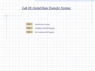
Lab 10 :Serial Data Transfer System: Slide 2 Asynchronous Inputs. Slide 3 Loadable 4-Bit Shift Register. Slide 4 Re-circulating Shift Register
5V 0 1 0 Pre D Q AMBIGOUS! D and Clock control Q. 0 1 0 >Clk Q 5V Clr R 5 millisec. 0 1 0 C 1 0 Lab 10 : Asynchronous inputs : All flip flops have 2 additional inputs called “Asynchronous Inputs” (Pre and Clr). They allow the user to set initial conditions at Q. Pre is called the pre- set input. Connecting it to 0 sets Q to 1. Clr is called the clear input. Connecting it to 0 resets Q to 0. D and Clk control Q Pre and Clr are called asynchronous because they can be used to set and clear the flip flop without the need of a clock. D and Clk are called synchronous inputs. They need a clock signal to change Q. Pre and CLr override the conditions at the synch inputs (D and Clk) if they are left asserted (0). Pre = Clr =1 allows D and Clk to control Q. Pre = Clr =0 is not allowed … or … AMBIGUOUS Pre and Clr can be used to set initial conditions at Q. Here is a “Power On Reset” circuit that ensures the flip flop starts at Q=0 when power is first applied to the flip flop. When the power is first applied to the circuit the capacitor is uncharged (0V) and grounds the Clr input. Clr=0 clears the flip flop! The cap charges to 5V through the resistor. The RC time constant determines the amount of time it takes for the capacitor to charge up. Assume that RC is chosen so that it takes 5 milliseconds to charge the capacitor. Clr will clear the flip flop for 5 milliseconds after the power is applied to the circuit. Once the cap is charged then Clr=1 and Q can be controlled by D and Clk. Slide #2
Step 4 : Provide a 4th clock pulse. Step 3 : Provide a 3rd clock pulse. Step 2 : Apply 0 to Load. 0 Step 2 : Provide a 2nd clock pulse. Step 2 : Provide a 2nd clock pulse. Load A B C 1 0 1 0 0 0 1 D Step 1 : Provide a clock pulse. Step 1 : Provide a clock pulse. Step 4 : Provide a 4th clock pulse. Step 3 : Provide a 3rd clock pulse. Step 1 : Apply 6 to inputs A, B, C, D 1 4-Bit 0 1 1 Din 0 >Clk QA QB QC QD 0 0 0 0 0 1 1 1 1 1 0 0 1 1 1 1 0 0 0 1 0 1 1 1 0 0 1 0 1 1 1 0 Lab 10 : Loadable 4-Bit Shift Register : A 4-bit number can be loaded into the shift register (via inputs A, B, C, D and Load). The number can be shifted from output QA to QB to QC to QD. The shift register will be loaded with the number 6. Shift the number: Load is connected to 1. This enables the shift register to shift the number. Din is connected to 1. Din is the data input to QA. The data at QA will shift right to QB. The data at QB shifts to QC.QC shifts to QD. You have seen how it takes 4 clock pulses to move the number 6 out of the shift register and fill it with 1’s from the Din input. Din will be connected to 0. This will shift the 1’s out and fill the shift register with 0’s. 1 0 1 Slide #3
1 Load A B C D 4-Bit Din 1 0 1 1 0 0 >Clk 1 0 0 1 QA QB QC QD 1 1 0 0 0 0 1 0 1 0 0 0 0 1 0 1 0 1 Lab 10 : Re-circulating Shift Register. The loadable shift registercan be configured as a re-circulatingshift register. You must connect the last stage of the shift register (QD) to the data input (Din). The connection from QD output to Din data input creates a loop or a ring. The shift register will be loaded with the number 9. To re-circulate the number: Apply 4 clock pulses. 0 Slide #4