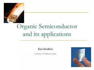
Organic Semiconductor
Organic Semiconductor. Gaojie Lu ECE423 Presentation 12-16-2006. Outline For Organic Semiconductor. Introduction to Organic Semiconductor Relation of Organic Semiconductors to Inorganic Characteristics of Organic Semiconductor Organic Semiconductor Devices Future Applications Summary.

Organic Semiconductor
E N D
Presentation Transcript
Organic Semiconductor Gaojie LuECE423 Presentation12-16-2006
Outline For Organic Semiconductor • Introduction to Organic Semiconductor • Relation of Organic Semiconductors to Inorganic • Characteristics of Organic Semiconductor • Organic Semiconductor Devices • Future Applications • Summary
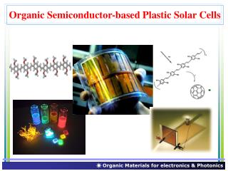
Introduction to Organic Semiconductor • Introduction to Organic Semiconductor • Organic Semiconductors are semiconductors which use organic molecules rather than silicon for their active material. This active material can be composed of a wide variety of molecules • Low cost of the technology • Compatibility with plastic substances • Lower temperature manufacturing (60-120° C) • Possible to achieve flexible structures • Low voltages, comparable with the performance for solution monitoring and some innovative applications
Also studied for more than 50 years Huge variety of choices for organic molecules for use in semiconductors Charge transport significantly different Usually comprised of many individual molecules held together by Van der Waals forces Many different fabrication techniques on different substrates Relation of Organic Semiconductors to Inorganic C60
Generally operate under accumulation mode, not inversion mode Relation of Organic Semiconductors to Inorganic Cont.
Mobilities of organic semiconductors have improved by five orders of magnitude over the past 15 years. Large research efforts using materials such as these led to some of this increase.
Organic Semiconductors Device-OLED • An organic light-emitting diode (OLED) is a special type of light-emitting diode (LED) in which the emissive layer comprises a thin-film of certain organic compounds. The emissive electroluminescent layer can include a polymeric substance that allows the deposition of very suitable organic compounds • For example, in rows and columns on a flat carrier by using a simple "printing" method to create a matrix of pixels which can emit different colored light.
TFTs are transistors created using thin films, usually of silicon deposited on glass. The deposited silicon must be crystallized using laser pulses at high temperatures. For organics to compete with a-S:H, their mobility should be greater than 0.1 cm²/V s and their on/off current ratio of greater than 106 OTFTs active layers can be thermally evaporated and deposited at much lower temperatures (i.e. 60° C) Organic Semiconductors Device-OTFT
Benefits Does not require a glass substrate as amorphous silicon does Low temperature manufacture Could be made on a piece of plastic Deposition techniques could reduce costs dramatically Challenges Workarounds for complications with photoresists Finding organic semiconductors with high enough mobilities & switching times Organic TFT Tightness
Future Outlook • OTFTs for active-matrix displays • Flexible view screens (or anything…) • New generations of smart cards • Organic smart pixels with OLEDs • Large-area display electronics • Organic semiconductor advances in mobility, switching time, and manufacturing may lead to many possibilities
References • H. E. Katz, Z. Bao, and S. J. Gilat, J. Acc. Chem. Res., vol.34, pp.359, 2001. • Nandita Madhavan, “Small-molecule organic semiconductors,” April 01, 2002. • A. Dodabalapur, “The future of organic semiconductor devies,” Device Research Conference 2000, Conference Digest, pp. 11-14, June 2000. • http://assets.cambridge.org/052182/3307/excerpt/0521823307_excerpt.pdf • http://www.aist.go.jp/aist_e/latest_research/2004/20041118/20041118.html • [11] C. D. Dimitrakopoulos and D. J. Mascaro, “Organic thin-film transistors: A review of recent advances,” IBM J. Res. & Dev. Vol. 45, No. 1, Jan. 2001. • [12] C. Reese, M. Roberts, M. M. Ling and Z. Bao, “Organic thin film transistors,” materialstoday, pp.20-27, Sept. 2004. • [13] Y. Inoue, et al., “Organic Thin-file transistors with high electron mobility based on perfluoropentacene,” Japan Society of Applied Physis, Vol. 44, No. 6A pp. 3663-3668, 2005 • Gao Z Q, Lee C S, Bello I, Lee S T, Chen R M, Luh T Y, Shi J and Tang C W 1999 Appl. Phys. • Lett. 74, 865 • Kulkarni A P, Gifford A P, Tonzola C J and Jenekhea S A 2005 Appl. Phys. Lett. 86, 061106-1 • Shi J M and Tang C W 2002 Appl. Phys. Lett. 80, 3201 • Gebeyehu D, Walzer K, He G, Pfeiffer M, Leo K, Brandt J, Gerhard A, Stössel P and Vestweber H • 2005 Synth. Met. 148, 205 • Hosokawa C, Higashi H, Nakamura H and Kusumoto T 1995 Appl. Phys. Lett. 67, 3853 • Liao C H, Lee M T, Tsai C H and Chen C H 2005 Appl. Phys. Lett. 86, 203507 • Wu Y Z, Zheng X Y, Zhu W Q, Sun R G, Jiang X Y, Zhang Z L and Xu S H 2003 Appl. Phys. • Lett. 83, 5077 • Morin J F, Leclerc M, Adès D and Siove A 2005 Macromol. Rapid Commun. 26, 761 • http://www.oea-osc.com/persp_overview.htm • http://www.phys.unsw.edu.au/~arh/background/Organic%20Electronics/Organics.html • http://pubs.acs.org/hotartcl/ci/00/apr/0650wallace.html • http://www.drproctor.com/os/ • www.st-andrews.ac.uk/~osc/org-semi.html • A.Tsumura, H. Koezuka, T. Ando,Appl.Phys.Lett. 49 (1986) 1210 • G. Horowitz, X. Peng, D. Fichou, F. Garnier. J.Appl.Phys. 67 (1989) 528 • S. R. Forrest, Nature 428, 911 (2004). • T. Tsujimura, SID 2003 Technical Digest Vol.XXXIV, • N. Greenham and R. H. Friend, in Solid State Physics: Advances in Research and Applications, Vol. 49, H. Ehrenreich and F. Spaepen, Eds., Academic Press, San Diego, 1995, pp. 1–149. • A. J. Lovinger and L. J. Rothberg, “Electrically Active Organic and Polymeric Materials for Thin-Film- Transistor-Applications,” J. Mater. Res. 11, 1581 (1996). • N. Hirohata, T. Tada and S. Yagyu: Proc. Int. Display Workshop 2004(IDW’04), p. 355. • Baude, P. F., et al., Appl. Phys. Lett. (2003) 82 (22), 3964 • Kelley, T. W., et al., Mater. Res. Soc. Symp. Proc. (2003) 771, 169 • Sundar, V. C., et al., Science (2004) 303, 1644 • Dimitrakopoulos, C. D., and Malenfant, P. R. L., Adv. Mater. (2002) 14 (2), 99 • Kagan, C. R., Thin Film Transistors, Marcel Dekker Inc., New York, (2003) • Zhang, J., et al., Appl. Phys. Lett. (2004) 84 (1), 142 • Yuan, J., et al., Appl. Phys. Lett. (2003) 82 (22), 3967 • Bao, Z., et al., Appl. Phys. Lett. (1996) 69 (20), 3066 • Lin, Y.-Y., et al., IEEE Trans. Electron Dev. (1997) 44 (8), 1325 • Katz, H. E., J. Mater. Chem. (1997) 7 (3), 369 • Park, S. K., et al., IEEE Trans. Electron Dev. (2002) 49 (11), 200822. Malenfant, P. R. L., et al., Appl. Phys. Lett. (2002) 80