Organic Semiconductor-based Plastic Solar Cells
Organic Semiconductor-based Plastic Solar Cells. What’s PVs. Light energy (photons). Electrical energy.

Organic Semiconductor-based Plastic Solar Cells
E N D
Presentation Transcript
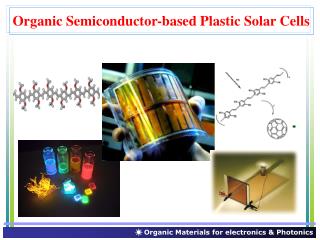
Organic Semiconductor-based Plastic Solar Cells Organic Materials for electronics & Photonics
What’s PVs Light energy (photons) Electrical energy When sunlight is absorbed by some materials, the solar energy knocks electrons loose from their atoms, allowing the electrons to flow through the material to produce electricity. This process of converting light (photons) to electricity (voltage) is called thephotovoltaic (PV) effect. Organic Materials for electronics & Photonics
Solar energy At earth’s surface average solar energy is ~ 4 x 1024 J / year Global energy consumption (2001) was ~ 4 x 10²⁰ J / year (increasing ~ 2% annually) Source: DOE (U.S. Department of Energy) Source:N. Lewis (Caltech) In US, average power requirement is 3.3 TW. With 10% efficient cells we would need 1.7% of land area devoted to PV (~ area occupied by interstate highways) Organic Materials for electronics & Photonics
1839 : Finding of Photovoltaic effect with liquid (Edmond becquerel) 1876 : Photovoltaic effect in a solid (Heinrich Hertz) 1883 : Se solar cell (C. Fritts) 1930 : Research of Cu2O/Cu solar cell 1941 : Patent of Si solar cell (R. Ohl) 1954 : Crystalline Si solar cell (Bell Lab.) ; 4 % efficiency 1958 : Using as assistant power in the spaceship (Vanguard I ) ; 5 mW 1973 : oil crisis 1980 : solar cell using CdTe, CuInSe2 ,TiO2 etc. 1997 : world product 100MWp 2000 : research of an advanced materials and structures (dye sensitized solar cell, organic solar cell) cheap process , flexible substrate History Organic Materials for electronics & Photonics
h (photon) Metal top electrode n-type Semiconductor p-type Semiconductor Metal back contact Space charge region Photovoltaic (PV) effect In a conventional semiconductor, light absorption generates an electric field that separates the photo-induced charges.Ec and Ev are the energies at the conduction and valence bands, respectively. Organic Materials for electronics & Photonics
Cell efficiency ISC : Short-circuit current Current value when V = 0 VOC : Open-circuit voltage Voltage value when I = 0 P : Power output of the cell P = IV F.F : Fill factor < Power conversion efficiency (η) > < Incident-photon-to-current conversion efficiency (IPCE) > Under AM 1.5G simulated solar illumination Organic Materials for electronics & Photonics
Air mass (AM) θz Organic Materials for electronics & Photonics
Sunlight spectrum Global condition (G) : including the diffusion component (indirect component owing to scattering and reflection in the atmosphere and surrounding landscape) Direct condition (D) : without the diffusion component Organic Materials for electronics & Photonics
태양전지 실리콘 반도체 화합물 반도체 기타 염료감응태양전지 결정계 비결정계 II•VI족 CdS CdTe… III•V족 GaAs InP… I•III•VI족 CuInSe2.. 유기태양전지 단결정 다결정 Classification Conventional inorganic p/n junction solar cell Organic Materials for electronics & Photonics
Progress of cell efficiencies Under AM 1.5G simulated solar illumination Organic Materials for electronics & Photonics
PV systems installed in Korea Organic Materials for electronics & Photonics
PV systems installed in Korea Organic Materials for electronics & Photonics
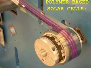
Why OPVs? Advantages of Organic PVs (OPVs) -Processed easily over large area using -spin-coating -doctor blade techniques (wet-processing) -evaporation through a mask (dry processing) -printing -Low cost -Low weight -Mechanical flexibility and transparency -Band gap of organic materials can be easily tuned chemically by incorporation of different functional group Organic Materials for electronics & Photonics
US$ 0.10/W US$ 0.20/W US$ 0.50/W 100 80 Efficiency (%) 60 3-1 Thermodynamic limit US$ 1.00/W 40 3 3-2 20 US$ 3.50/W 1 2 100 300 400 500 200 Cost (US$/m2) Why OPVs? The concept of third-generation PV technologies, originally developed by Martin Green of the University of New South Wales 1: PV cell based on silicon wafers 2: thin-film technology 3: high-efficiency thin-film technology using concepts such as hot carriers, multiple electron–hole pair creation, and thermophotonics Cost-efficiency analysis for first-, second-, and third-generation PV technologies ( labeled 1, 2, and 3, respectively). Region 3-1 depicts very-high-efficiency devices that require novel mechanisms of device operation. Region 3-2(the region in which organic PV devices lie) depicts devices with moderate efficiencies and very low costs. Organic Materials for electronics & Photonics
Why OPVs? Source: Siemens AG Organic Materials for electronics & Photonics
Why OPVs? (Application) Organic Materials for electronics & Photonics
Why OPVs? (Application) Organic Materials for electronics & Photonics
Requirement of OPVs Source: Siemens AG Organic Materials for electronics & Photonics
History of OPVs Organic Materials for electronics & Photonics
e- hv D metal A ITO h+ PV effect in conjugated polymer • Light is absorbed in the polymer layer • Absorption creates a bound electron-hole pair (exciton) • Exciton is split into separate charges which are collected at contacts • Exciton must be seperated so that a photocurrent can be collected. • Excitons dissociated by electron transfer to an acceptor material, or hole transfer to a donor. • Simplest approach is to make a donor-acceptor heterojunction Organic Materials for electronics & Photonics
Exciton : generation & separation Excitons are produced in a conducting polymer. An incident photon produces bound electron–hole pairs called excitons, which transport charges in photovoltaic polymers. Excitons dissociate at interfaces between materials having different ionization energies and electron affinities Organic Materials for electronics & Photonics
Photo-induced charge transfer • Photon absorption (A) Exciton generation by absorption of light • Exciton diffusion (ED) Exciton diffusion over ~LD (~20 nm) • Charge-transfer reaction (CT) Exciton dissociation by rapid and efficient charge transfer • Collection of the carriers (CC) Charge extraction by the internal electric field CT CC A ED cathode anode donor acceptor EQE: external quantum efficiency IQE: internal quantum efficiency EQE = AIQE = AEDCTCC Organic Materials for electronics & Photonics
Device architecture Top electrode • Single-layer • Bilayer • Bulk heterojunction Active layer ITO glass Single-layer PV cell Bilayer PV cell Bulk heterojunction PV cell Organic Materials for electronics & Photonics
Organic or polymer single-layer PVs Disadvantage Organic Materials for electronics & Photonics
Single-layer PVs Organic single crystals Organic Materials for electronics & Photonics
Low efficiency Limitation of single-layer PVs High exciton binding energy Low bipolar mobility in one molecule Organic Materials for electronics & Photonics
Organic or polymer bilayer PVs • Charge transfer can occur between two semiconductors with offset energy levels. • Excitons can diffuse approximately 10 nm to an interface. (less than 20 nm) • A film thickness of approximately 100 nm is needed to absorb most of the light. • Polymer bilayer cell showed 1.9 % energy conversion efficiency. • Small molecule bilayer cell showed 3.6 % power conversion efficiency with 3 layers. Organic Materials for electronics & Photonics
Bilayer PVs Small molecular organic bilayer PV cell Improving molecular PV cell Organic Materials for electronics & Photonics
Limitation of organic or polymer bilayer PVs Organic Materials for electronics & Photonics
Bulk heterojunction (BHJ) PVs Organic Materials for electronics & Photonics
Device geometries Organic Materials for electronics & Photonics
Working principle of BHJ device 1. Incoming photons are absorbed ⇒ Creation of excitons on the Donor / Acceptor 2. Exciton is separated at the donor / acceptor interface ⇒ Creation of charge carriers 3. Charge carriers within drift distance reach electrodes ⇒ Creation of short circuit current ISC 1. The “photodoping” leads to splitting of Fermi levels ⇒ Creation of open circuit voltage VOC 2. Charge transport properties, module geometry ⇒ Fill factor FF Organic Materials for electronics & Photonics
Photoinduced charge generation Organic Materials for electronics & Photonics
Charge transfer Organic Materials for electronics & Photonics
Charge recombination Organic Materials for electronics & Photonics
3-D percolation Organic Materials for electronics & Photonics
3-D percolation - PL quenching Organic Materials for electronics & Photonics
3-D percolation - morphology and transport Organic Materials for electronics & Photonics
3-D percolation – morphology and transport Organic Materials for electronics & Photonics
Efficiencies Organic Materials for electronics & Photonics
Production Organic Materials for electronics & Photonics
Film preparation Organic Materials for electronics & Photonics
Film preparation Organic Materials for electronics & Photonics
Optimization for high efficiency 1. Conjugated polymer with low band gap Maximum photon flux of sun = 700 nm Eg= 1.24 / 0.7= 1.77 [eV] Maximum absorption of photon of sun Isc: tuning of the transport property (mobility); Optimization of cell geometry in dependence of the cell thickness Voc: tuning of the electronic energy level of the donor-acceptor system; Voc of ~2 V observed in polymeric donor- acceptor system F.F: tuning of the contacts and morphology: lowering of serial resistance 2. Bulk heterojunction morphology exciton diffusion length of conjugated polymer = below 20 nm 3. High carrier mobility electron and hole mobility of conjugated polymer Organic Materials for electronics & Photonics
O M e O Materials for BHJ organic solar cell PCBM MDMO-PPV F8BT P3HT CuPc pentacene TiO2 or ZnO nanoparticles C60 PFB Organic Materials for electronics & Photonics
O M e O • Polymer/PCBM interpenetrating system Voc = 0.82 V Jsc = 5.25 mA/cm2 FF = 0.61 AM1.5G = 2.5 % (under 80 mW/cm2) PCBM MDMO-PPV < S. E. Shaheen, et al., Appl. Phys. Lett. 1998, 395, 257 > A D Metal electrode LiF Active layer PEDOT:PSS ITO glass Donor/Acceptor composite solution Organic Materials for electronics & Photonics
Materials issue - matching the solar emission The flexibility in chemical tailoring is necessary for matching the absorption of the PV material to the solar emission spectrum. Organic Materials for electronics & Photonics
Bandgap engineering < The parameters determining the bandgap of conjugated polymers > E∆r : the energy contribution from bond length alternation RE : the resonance energy EΘ : the energy caused by the inter ring torsion angle ESUB : the influence of the substituents. EG = E△r + RE + Eθ + Esub 1. Aromatic form shows higher stabilization energy and therefore the higher bandgap. 2. Resonance energy leads to an energy stabilization and so to an increased splitting of the HOMO-LUMO energy. 3. Torsion between the ring plain interrupts the conjugation and therefore increases the bandgap. 4. Electron donating groups raise the HOMO level and electron withdrawing groups lower the LUMO. 5. In the solid phase, additional intermolecular effects between the chains have to be taken into account, which generally leads to broader bands and a lower bandgap. Organic Materials for electronics & Photonics
Synthetic strategy 1. Introduction of side groups: increase or decrease the electron density 2. Push-pull polymers: The bandgap of copolymers with alternating of electron rich and electron poor compounds can decrease significantly. (The bond length alternation is reduced and so the Peierls stabilisation.) 3. Introduction of methine groups between the ring systems: The quinoid form minimize the inter annular rotation by the double bond character of the bridge bonds as well as the bond length alternation . (The structure becomes more flat and the resonance between the rings is increased.) < Potential diagram vs. bond length alternation for (a) trans-polyacethylene as conjugated polymer with degenerate ground state; (b) for polyphenylene as conjugated polymer with nondegenerate ground state> Organic Materials for electronics & Photonics
Low bandgap polymer - PTPTB Poly-N-dodecyl-2,5-bis(2´-thienyl)pyrrole-2,1,3-benzothiadiazole: PTPTB the push-pull concept by altering electron rich N-dodecyl-2,5-bis(2´-thienyl)pyrrole and electron deficient 2,1,3-benzothiadiazole groups Voc = 720 mV ISC = 3 mA/cm2 FF = 0.38 η = 1 % Enhancement of absorption area Organic Materials for electronics & Photonics