Ideal Diode Equation
Ideal Diode Equation. Important Points of This Lecture. There are several different techniques that can be used to determine the diode voltage and current in a circuit Ideal diode equation

Ideal Diode Equation
E N D
Presentation Transcript
Important Points of This Lecture • There are several different techniques that can be used to determine the diode voltage and current in a circuit • Ideal diode equation • Results are acceptable when voltages applied to diode are comparable or smaller than the turn-on voltage and larger than about 90% of the breakdown voltage • Piecewise model • Results are acceptable when voltage applied to the diode are large in magnitude when comparised to the turn-on voltage
Embedded in the Ideal Diode Equation is dependences on • Temperature • Doping concentration of p and n sides • Semiconductor material • Bandgap energy • Direct vs. indirect bandgap • PSpice diode model using Ideal Diode Eq. • User can edit diode model • Diode model can also be more complex to include deviations from Ideal Diode Eq. such as frequency dependence of operation
P-N junctions • We already know that a voltage is developed across a p-n junction caused by • the diffusion of electrons from the n-side of the junction into the p-side and • the diffusion of holes from the p-side of the junction into the n-side
Reminder • Drift currents only flow when there is an electric field present. • Diffusion currents only flow when there is a concentration difference for either the electrons or holes (or both).
When the applied voltage is zero • The diode voltage and current are equal to zero on average • Any electron that diffuses through the depletion region from the n-side to the p-side is counterbalanced by an electron that drifts from the p-side to the n-side • Any hole that diffuses through the depletion region from the p-side to the n-side is counterbalanced by an electron that drifts from the n-side to the p-side • So, at any one instant (well under a nanosecond), we may measure a diode current. This current gives rise to one of the sources of electronic noise.
Applied voltage is less than zero • The energy barrier between the p-side and n-side of the diode became larger. • It becomes less favorable for diffusion currents to flow • It become more favorable for drift currents to flow • The diode current is non-zero • The amount of current that flows across the p-n junction depends on the number of electrons in the p-type material and the number of holes in the n-type material • Therefore, the more heavily doped the p-n junction is the smaller the current will be that flows when the diode is reverse biased
Applied Voltage is greater than zero • The energy barrier between the p-side and n-side of the diode became smaller with increasing positive applied voltage until there is no barrier left. • It becomes less favorable for drift currents to flow • There is no electric field left to force them to flow • There is nothing to prevent the diffusion currents to flow • The diode current is non-zero • The amount of current that flows across the p-n junction depends on the gradient of electrons (difference in the concentration) between the n- and p-type material and the gradient of holes between the p- and n-type material • The point at which the barrier becomes zero (the flat-band condition) depends on the value of the built-in voltage. The larger the built-in voltage, the more applied voltage is needed to remove the barrier. • It takes more applied voltage to get current to flow for a heavily doped p-n junction
Ideal Diode Equation • Empirical fit for both the negative and positive I-V of a diode when the magnitude of the applied voltage is reasonably small.
Ideal Diode Equation Where IDand VD are the diode current and voltage, respectively q is the charge on the electron n is the ideality factor: n = 1 for indirect semiconductors (Si, Ge, etc.) n = 2 for direct semiconductors (GaAs, InP, etc.) k is Boltzmann’s constant T is temperature in Kelvin kT is also known as Vth, the thermal voltage. At 300K (room temperature), kT = 25.9meV
Simplification • When VD is negative • When VD is positive
To Find n and Io • Using the curve tracer, collect the I-V of a diode under small positive bias voltages • Plot the I-V as a semi-log • The y-intercept is equal to the natural log of the reverse saturation current • The slope of the line is proportional to 1/n
Questions • How does the I-V characteristic of a heavily doped diode differ from that of a lightly doped diode? • Why does the I-V characteristics differ? • For any diode, how does the I-V characteristic change as temperature increases? • For the same doping concentration, how does the I-V characteristic of a wide bandgap (Eg) semiconductor compare to a narrow bandgap semiconductor (say GaAs vs. Si)?
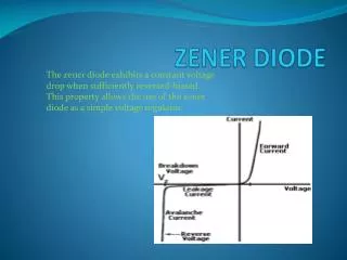
What the Ideal Diode Equation Doesn’t Explain • I-V characteristics under large forward and reverse bias conditions • Large current flow when at a large negative voltage (Breakdown voltage, VBR) • ‘Linear’ relationship between ID and VD at reasonably large positive voltages (Va > Vbi)
Nonideal (but real) I-V Characteristic • Need another model • Modifications to Ideal Diode Equation are used in PSpice • We will use a different model called the Piecewise Model
PSpice • Simplest diode model in PSpice uses only the ideal diode equation • More complex diode models in PSpice include: • Parasitic resistances to account for the linear regions • Breakdown voltage with current multipliers to map the knee between Io and the current at breakdown • Temperature dependences of various parameters • Parasitic capacitances to account for the frequency dependence
Capture versus Schematics • It doesn’t matter to me which you use • I find Schematics easier, but the lab encourages the use of Capture


