Chapter 11 BJT Static Characteristics
Chapter 11 BJT Static Characteristics. Chapter 11. BJT Static Characteristics. Ebers -Moll Model. The Ebers-Moll model is a large-signal equivalent circuit which describes both the active and saturation regions of BJT operation.

Chapter 11 BJT Static Characteristics
E N D
Presentation Transcript
Chapter 11 BJT Static Characteristics
Chapter 11 BJT Static Characteristics Ebers-Moll Model • The Ebers-Moll model is a large-signal equivalent circuit which describes both the active and saturation regions of BJT operation. • This model is to be used to calculate IC, IE for given VBE, VBC. IRO IFO • If only VEB is applied (VCB = 0): • If only VCBis applied (VEB = 0):
Chapter 11 BJT Static Characteristics Ebers-Moll Model • Reciprocity relationship: aR : reverse common base gain aF : forward common base gain • In the general case, when VEB and VCB are non-zero:
Deviations from the Ideal Chapter 11 BJT Static Characteristics • Common base Deviations, due to model limitations • Common emitter
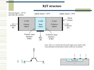
Chapter 11 BJT Static Characteristics W IE IC P+ N P + VEB Base-Width Modulation • Common-Emitter ConfigurationActive Mode Operation • Recalling two formulas, DpB(x) • If –VCB increases • W decreases • bdc increases • IC increases (VCB=0) Increasing –VCB x W 0
Chapter 11 BJT Static Characteristics Punch-Through • Punch-Through: E-B and C-B depletion regions in the base touch each other, so that W = 0. • As –VCB increases beyond the punch-through point, the E-B potential hill decreases and therefore increases the carrier injections and IC. WB=xnEB+xnCB
Chapter 11 BJT Static Characteristics Breakdown Mechanisms • In the common-emitter configuration, for high output voltage VCE, the output current IC will increase rapidly due to the two mechanisms: punch-through and avalanche. Punch-through Avalanche Increasing reverse bias of C-B junction
Chapter 11 BJT Static Characteristics Avalanche Multiplication • Holes [0] are injected into the base [1], then collected by the C-B junction. • Some holes in the C-B depletion region have enough energy do impact ionization [2]. • The generated electrons are swept into the base [3], then injected into the emitter [4]. • Each injected electron results in the injection of IEp/IEn holes from the emitter into the base [5]. pnp BJT • For each pair created in the C-B depletion region by impact ionization, (IEp/IEn) +1>bdc additional holes flow into the collector. • This means that carrier multiplication in C-B depletion region is internally amplified. M : multiplication factor
Chapter 11 BJT Static Characteristics Geometrical Effects • Emitter area is not equal to collector area. • Current does not flow in one direction only. • Series resistance. • Voltage drop occurs not only across the junction. • Current crowding. • Due to lateral flow, current is larger around emitter periphery than the collector periphery.
Chapter 11 BJT Static Characteristics Graded Base • Dopants are injected through diffusion. • More or less falling exponential distribution with distance into beneath of the semiconductor. • The doping within the base is not constant as assumed in ideal analysis. • A function of position, having maximum at E-B junction and minimum at C-B junction. • Creating a built-in electric field. • The electric field enhances the transport of minority carrier across the quasineutral width of the base. • Increase of IE and IC. xdiff : exponential decay constant
Chapter 11 BJT Static Characteristics Figures of Merit Due to recombination in emitter depletion region Gummel Plot Due to high level injection in base, base series resistance, and current crowding
Chapter 11 BJT Static Characteristics Polysilicon Emitter BJT • bdc is larger for a poly-Si emitter BJT as compared with an all-crystalline emitter BJT. • This is due to reduced dpE(x)/dx at the edge of the emitter depletion region. Lower mp • Continuity of hole current in emitter Shallower slope less JP higher g, b
Chapter 11 BJT Static Characteristics Summary on BJT Performance • High gain (bdc >> 1) • One-sided emitter junction, so that emitter efficiency g 1 • Emitter doped much more heavily than base (NE >> NB). • Narrow base, so base transport factor aT 1. • Quasi-neutral base width << minority-carrier diffusion length(W << LB). • IC determined only by IB (IC function of VCE or VCB) • One-sided collector junction, so that quasineutral base width W does not change drastically with changes in VCE or VCB. • Base doped more heavily than collector (NB > NC), W = WB – xnEB – xnCB for pnp BJT.