chapter 2 transistors (BJT)
chapter 2 transistors (BJT). 2.1 Transistor classification 2.2 Bipolar junction transistors (BJT) construction 2.3 Transistor action and operating 2.4 Quiescent Operating Point 2.5 Bipolar transistor characteristics 2.6 Transistor parameters 2.7 Current gain
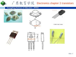

chapter 2 transistors (BJT)
E N D
Presentation Transcript
chapter 2 transistors (BJT) • 2.1 Transistor classification • 2.2 Bipolar junction transistors (BJT) construction • 2.3 Transistor action and operating • 2.4 Quiescent Operating Point • 2.5 Bipolar transistor characteristics • 2.6 Transistor parameters • 2.7 Current gain • 2.8 Typical BJT characteristics and maximum ratings • 2.9 Transistor operating configurations
exercise • 1.Explain,with the aid of sketches,the operation • Of an n-p-n transistor and also explain why the • Collector current is very nearly equal to the emitter • current. • 2.Describe the basic principle of operation of a • Bipolar junction transistor,including why majority • carriers crossing into the base from the emitter • Pass to the collector and why the collector current • Is almost unaffected by the collector potential.
3.Explain what is meant by ‘leakage current’ in a • Bipolar junction transistor and why this can usually • beignored. • 4.For a transistor connected in common-emitter • configuration,sketch the typical output characteristics • Relating collector current and the collector-emitter • voltage,for various values of base current.Explain • The shape of the characteristics.
5.Sketch the typical input characteristic relating base • Current and the base-emitter voltage foratransist or • Connected incommon-emitter configuration and • Explain its shape. • 6.With the aid of a circuit diagram,explain how • The input and output characteristic of a common- • Emitter n-p-n transistor may be produced. • 7.Define the term ‘current gain’for a bipolar junction • Transistor operating incommon-emitter mode.
8.Abipolar junction transistor operates with a col- • Lector current of 1.2A and abase current of 50mA. • What will the value of emitter current be? • [1.25A] • 9.What is the value of common-emitter current • gain for the transistor in problem 8? [24]
chapter 2 transistors (F.E.T) • 3.0 Exercise • 3.1 Field effect transistor classification • 3.2 Field effect transistor construction • 3.3 N-type junction field effect transistor operating • 3.4 Field effect transistor characteristics • 3.5 Typical F.E.T. characteristics and maximum ratings • 3.6 M-O-S field effect transistor
Field effect transistors are available in two basic forms; • Junction gate and insulated gate. The gate source junction • Of a junction gate field effect transistor(JFET) is effectively are verse-biased p-n junction.The gate connection • Of an insulated gate field effect transistor(IGFET).
3.2 The junction field-effect transistor(j.f.e.t.) • Figure Conformation of N channel J.F.E.T
N channel JFET • P channel JFET • Figure Symbol of JFET
3.3 The junction field-effect transistor operating • Figure Operation of N channel JFET
3.6 Metal-oxide-semiconductor field-effect transistor 3.6.1 depletion-type MOS FET Construction of N channel depletion-type MOS FET • N channel • P channel
3.6 Metal-oxide-semiconductor field-effect transistor 3.6.2 Enhancement-type MOS FET • N channel • P channel Construction of N channel enhancement-type MOS FET • Figure depletion-type MOS FET
Assignment 1 • Tasks: • (Pass Criterion 2.1) Analyse the operation of different types of amplifier. In the wireless receiver customer provided, the audio-frequency input stage amplifier and the audio-frequency power amplifier are given below. • (Ⅰ)The audio-frequency input stage amplifier is show in figure 1.1. The relationships between collector current and collector voltage, with fixed values of base current, are given in table 1.1. You should make IEQ=4mA through adjusting R5, and take this point as its quiescent operating point, then measure the value of R5 and VCEQ. • (ⅰ) Draw the static output characteristics of the transistor, use these to determine the d.c. current gain and the a.c. current gain at the quiescent operating point. • (ⅱ) The resistance value of the load is vague with age. You should choose a certain value between 1.2 KΩ to 3 KΩ and draw the d.c. load line and a.c. load line at the static output characteristics. • (ⅲ) According to the a.c. load line, determine the maximum non-distortion voltage value of the a.c. output signal.