Bipolar Junction Transistors
A very gentle intro. Bipolar Junction Transistors. The invention that changed everything…. The real thing. Circuit diagram symbol. What transistors are good for. ~731M transistors in Intel core i7. Transistor action: BJT. BJT = B ipolar J unction T ransistor


Bipolar Junction Transistors
E N D
Presentation Transcript
A very gentle intro Bipolar Junction Transistors
The invention that changed everything… The real thing Circuit diagram symbol
What transistors are good for ~731M transistors in Intel core i7
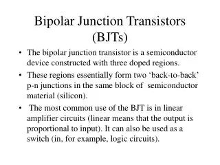
Transistor action: BJT BJT = Bipolar Junction Transistor Goal: control current flow from collector to emitter via base Fluid Analogy: Small signal controls a much larger signal
Transistor action:electron flow N - Emitter - For conventional current flow (tracking positive charge movement), flip the arrows! P - Base - - - Collector N
Bipolar Transistor Parameters BE: fwd bias BC: rev bias
IB Input characteristic Transistor ON Fwd biased diode Working on the steep part of the curve (blue dotted box highlights normal operating range) DVBE small DIB relatively large * Rule of thumb: use VBE ~ 0.7V when designing BJT circuits DIB DVBE
Output Characteristic Active region (light blue): Ic = bIB Ic~independent of VCE Saturation (yellow-ish): Icdepends on VCE and IB 0.3V
Load Line 1. KVL in loop through transistor give us the load line 2. One point for saturation: VCE = 0, Ic is maxed 3. One point for cutoff : Ic = 0, VCE is maxed 4. Operating point: intersection of load line and characteristic curve
Load Line Example VCC = 10 V RL = 400W VLED= 1.6 V (red) Assume IB = 200 mA 1. 0 = VCC – VLED – ICRL – VCE 2. VCE = 0 IC =(VCC– VLED)/RL = 21.0 mA 3. IC= 0 VCE= VCC - VLED = 8.4 V
Load Line for example circuit • Actual current will be about 18 mA, a little less than designed for, but not bad!
Image credits • http://www.st-andrews.ac.uk/~www_pa/Scots_Guide/info/comp/active/BiPolar/bpcur.html • http://www.electronics-tutorials.ws/transistor/tran_2.html