Bipolar Junction Transistors
Bipolar Junction Transistors. C. BJTs. B. E. Transistors. They are unidirectional current carrying devices like diodes with capability to control the current flowing through them Bipolar Junction Transistors ( BJT ) control current by current


Bipolar Junction Transistors
E N D
Presentation Transcript
Bipolar JunctionTransistors C BJTs B E
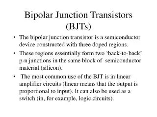
Transistors • They are unidirectional current carrying devices like diodes with capability to control the current flowing through them • Bipolar Junction Transistors (BJT) control current by current • Field Effect Transistors (FET) control current by voltage • They can be used either as switches or as amplifiers
A transistor allows you to controlthe current, not just block it in one direction. • A good analogy for a transistor is a pipe with an adjustable gate. • A transistor has three terminals. • The main path for current is between the collector and emitter. • The base controls how much current flows, just like the gate controls the flow of water in the pipe.
BIPOLAR JUNCTION TRANSISTOR • Two back to back P-N junctions • Emitter • Heavily doped • Main function is to supply majority carriers to base • Base • Lightly doped as compared to emitter • Thickness 10-6 m • Collector • Collect majority carriers from emitter through base • Physically larger than the emitter region N P N P P N C C E E B B
The BJT – Bipolar Junction Transistor The Two Types of BJT Transistors npn pnp n p n p n p E C E C C C Cross Section Cross Section B B B B Schematic Symbol Schematic Symbol E E
STRUCTURE • The collector surrounds the emitter region, making it almost impossible for the electrons injected into the base region to escape being collected, thus making the resulting value of α very close to unity, and so, giving the transistor a large β
Energy Band diagram of an unbiased transistor • N-region moves down and P-region moves up due to diffusion of majority carriers across junction. • The displacement of band and carrier migration stops when Fermi levels in the three regions are equalized Biasing of Transistor • Base and emitter current when collector is open • EB is forward biased- electron diffusion from emitter to base and hole diffusion from base to emitter • Hence IB will be large and is equal to IE • Collector is open so no current flows into collector
Base and Collector current when the Emitter is open (ICBO) • CB is reverse biased- electron from base flow into collector region and holes from collector flow into base • This current is known as reverse saturation current • The base current IB will be small and is equal to ICBO
Four Ways of Transistor biasing • Both EB and CB junctions are fwd biased- Huge current flows through base. The transistor is said to be operating in Saturation region (mode) • Both EB and CB junctions are reverse biased- The transistor is said to be operating in cut off region (mode) • EB junction is fwd biased and CB junction is reverse biased. The collector current is controlled by emitter current or base current- The transistor is said to operate in Active region (mode) • EB junction in reverse biased and CB junction in fwd biased- inverted region (mode)
Transistor Biasing-Active RegionWhen both Emitter and Collector are closed • Emitter-base junction is forward biased • Collector-base junction is reverse biased • DC emitter supply voltage (VEE)- Negative terminal of VEE is connected to emitter • DC collector supply voltage (VCC)- Positive terminal of VCC is connected to collector • IB becomes very small and IC will be as large as IE IE IC N P N VEE VCC IB
Transistor currents • Forward biasing from base to emitter narrows the BE depletion region • Reverse biasing from base to collector widens the depletion CB region • Conduction electrons diffuse into p-type base region • Base is lightly doped and also very thin- so very few electron combine with available hole and flow out of the base as valence electrons (small base electron current) IE IC N P N VEE VCC IB
Sufficient holes are not avail in base – remote possibility of joining of electrons with holes • Electron concentration is large on emitter side and nil on collector • Electrons swiftly move towards collector • At CB junction they are acted upon by strong electric field due to reverse bias and are swept into collector
Transistor currents • Most of the electrons diffuse into CB depletion region • These electrons are pulled across the reverse biased CB junction by the attraction of the collector supply voltage and form the collector electron current. Therefore IE= IC + IB • 1-2% of emittercurrent goes to supply base current and 98-99% goes to supply collector current • Moreover, IE flows into the transistor and IB & IC flow out of transistor • Current flowing in is taken as positive and currents flowing out are taken as negative • The ratio of the number of electrons arriving at collector to the number of electrons emitted by the emitter is called base transportation factor
Important Biasing Rule • Both collector and base are positive with respect to emitter • But collector is more positive than base • Different potentials have been designated by double subscripts as shown in the figure • VCB (Collector is more positive than base) and VBE (base is more positive than emitter) ++ C E C ++ - B + VCB + VBE VCB - E VBE B
Transistor circuit configuration • There are of three types • Common base (CB) OR grounded base • Common emitter (CE) OR grounded emitter • Common collector (CC) OR grounded collector • Common is the term used to denote the electrode that is common to the input and output circuits and it is generally grounded • Common-Base Biasing (CB) : input = VBE & IE • output = VCB & IC • Common-Emitter Biasing (CE): input = VBE & IB • output = VCE & IC • Common-Collector Biasing (CC): input = VBC & IB • output = VEC & IE
Common Base Configuration • Input signal applied between emitter & base • Output is taken from collector & base • Ratio of collector current to emitter current is called dc alpha (dc) of a transistor E C ++ - + VBE VCB B
The subscript dc on signifies that this ratio is defined from dc values of IC and IE • There is also an ac which refers to the ratio of change in collector current to the change in emitter current • For all practical purposes dc= ac= • IE is taken as positive (flowing into transistor) and IC is taken as negative (flowing out of transistor) • is the measure of quality of a transistor- higher its values, better is the transistor • Value ranges from 0.95 to 0.999
Common Emitter Configuration • The input signal is applied between the base and emitter and the output signal is taken out from the collector and the emitter • Ratio of collector current to base current is called dc beta (dc) of a transistor C Relation between and - B + and E
using then becomes or or or Common Collector Configuration • The input signal is applied between the base and collector and the output signal is taken out from the emitter-collector circuit • Ratio of emitter current to base current is
Output current=(1+) x Input current From the figure Relation between transistor currents We know C and - B + because We get and E
Therefore • This shows that emitter current initiated by the forward biased emitter base junction is split into two parts • (1-)IE which becomes base current in the external circuit • IE which becomes collector current in the external circuit
Static Characteristics • Common Base Static characteristics • Input characteristics. IE varies with VBE when voltage VCB is held constant • VCB is adjusted with the help of R1 • VBE is increased and corresponding values of IE are noted • The plot gives input characteristics • Similar to the forward characteristics of P-N diode • This characteristics is used to find the input resistance of the transistor. Its value is given by the reciprocal of its slope Rin= VBE / IE
BJT Input Characteristics IE 8 mA 6 mA IC C E IE 4 mA + VCB VBE 2 mA VEE VCC R2 R1 B VBE 0.7 V
Static Characteristics • Common Base Static characteristics • Output characteristics. IC varies with VCB when IE is held constant • VBE is adjusted with the help of R2 and IE is held constant • VCB is increased and corresponding values of IC are noted • The plot gives output characteristics • Then IE is increased to a value little higher and whole process is repeated • The output resistance of the transistor is given by Rout= VCB / IC IC C E IE + VCB VBE VEE VCC R2 R1 B
BJT Output Characteristics • IC flows even when VCB=0 for different values of IE(due to internal junction voltage at CB junction) • IC flows even when IE=0 (Collector leakage current or reverse saturation current ICBO) • The output resistance is very high (500k) IC Active Region IE Saturation Region Cutoff IE = 0 VCB
Static Characteristics • It can be seen that IC flows even when VCB is zero • It is due to the fact that electrons are being injected into base due to forward biased E-B junction and are collected by collector due to action of internal junction voltage at C-B junction • Another important feature is that a small amount of collector current flows even when the emitter current IE is zero called collector leakage current (ICBO) • When VCB is permitted to increase beyond a certain value, IC increases rapidly due to avalanche breakdown • This characteristics may be used to find ac ac =IC/ IE
Common Emitter Configuration • Transistor is biased in active region • Called CE because emitter is common to both VBB and VCC • VBB forward biases the EB junction and VCC reverse biases the CB C IC IB B E VCE VBE VBB VCC R2 R1 B Common Emitter(CE) Connection LP4
Static Characteristics • Common Emitter Static characteristics • Input characteristics. IB varies with VBE when voltage VCE is held constant • VCE is adjusted with the help of R1 • VBE is increased and corresponding values of IB are noted • The plot gives input characteristics • Procedure is repeated for different (constant) values of VCE • This characteristics is used to find the input resistance of the transistor. Its value is given by the reciprocal of its slope Rin= VBE / IB
IB 8 mA 6 mA 4 mA 2 mA VBE 0.7 V
Static Characteristics • Common Emitter Static characteristics • Output characteristics. IC varies with VCE when IB is held constant • IB is held constant • VCE is increased and corresponding values of IC are noted • The plot gives output characteristics • Then IB is increased to a value little higher and whole process is repeated • The output resistance in this case is very less as compared to CB circuit and is given by Rout= VCE / IC
As VCE increases from zero, IC rapidly increases to saturation level for a fixed value of IB • IC flows even when IB=0 (Collector leakage current or reverse saturation current ICEO), the transistor is said to be cutoff • When VCB is permitted to increase beyond a certain value, IC increases rapidly due to avalanche breakdown • This characteristics may be used to find ac ac =IC/ IB IC Active Region IB VCE Saturation Region Cutoff Region IB = 0
Common Base where (Reverse saturation current) Therefore, in general Common Emitter
(Reverse saturation current) where Relationship between dc and dc and
Common Base Formulas IE IC C E RE RL IB VCB and VBE VEE VCC B Where VBE=0.3 V for Ge and 0.7 V for Si Generally VEE>>VBE so IE=VEE/RE
Common Emitter Formulas IC C IB E RB RL IE VCE and VBE VBB VCC B
DC and DC = Common-emitter current gain = Common-base current gain = IC = IC IB IE The relationships between the two parameters are: = = + 1 1 - Note: and are sometimes referred to as dc and dc because the relationships being dealt with in the BJT are DC.
BJT Example Using Common-Base NPN Circuit Configuration C • Given: IB = 50 A , IC = 1 mA • Find: IE , , and • Solution: • IE = IB + IC = 0.05 mA + 1 mA = 1.05 mA • = IC / IB = 1 mA / 0.05 mA = 20 = IC / IE = 1 mA / 1.05 mA = 0.95238 could also be calculated using the value of with the formula from the previous slide. = = 20 = 0.95238 + 1 21 IC VCB + _ IB B VBE IE + _ E
Transistor as an amplifier • An electronic circuit that causes an increase in the voltage or power level of a signal • It is defined as the ratio of the output signal voltage to the input signal voltage IE IC VEE VCC IB RL
In the figure we see that an output voltage is developed across RL • The dc voltage VEE is a fixed voltage and causes a dc current IE to flow through EB junction • When the ac voltage Vi is super-imposed on VEE, the emitter base voltage varies with time • Say if VEE =10V and the peak voltage of Vi is is 1V, the EB voltage swings from 9V to 11V • The causes corresponding variations in IE and IC which gives Vo • The emitter variation due to EB voltage variation can be expressed as
The collector current IC changes by • This current IC flows through RL causing a voltage drop • Hence as • Where riis very small (100 ) and RL is of the order of kilo-ohms. It means Vo is larger than Vi indicating that the transistor has amplified small Vi to a larger Vo
Problems • In the CE Transistor circuit VBB= 5V, RBB= 107.5 k, RCC = 1 k, VCC = 10V. Find IB, IC, VCE, and the transistor power dissipation
In the CE Transistor circuit shown earlier VBB= 5V, RBB= 107.5 k, RCC = 1 k, VCC = 10V. Find IB, IC, VCE, and the transistor power dissipation using the characteristics as shown below By Applying KVL to the base emitter circuit By using this equation along with the iB / vBE characteristics of the base emitter junction, IB = 40 A By Applying KVL to the collector emitter circuit By using this equation along with the iC / vCE characteristics of the base collector junction,iC = 4 mA, VCE = 6V
iB 100 A 0 5V vBE Transistor power dissipation = VCEIC = 24 mW We can also solve the problem without using the characteristics if and VBE values are known iC 100 A 10 mA 80 A 60 A 40 A 20 A 0 vCE Output Characteristics Input Characteristics