Chapter 7 Complementary MOS (CMOS) Logic Design
Chapter 7 Complementary MOS (CMOS) Logic Design. Microelectronic Circuit Design Richard C. Jaeger Travis N. Blalock. Chapter Goals. Introduce CMOS logic concepts Explore the voltage transfer characteristics of CMOS inverters Learn to design basic and complex CMOS logic gates

Chapter 7 Complementary MOS (CMOS) Logic Design
E N D
Presentation Transcript
Chapter 7Complementary MOS (CMOS) Logic Design Microelectronic Circuit Design Richard C. JaegerTravis N. Blalock Microelectronic Circuit Design, 4E McGraw-Hill
Chapter Goals • Introduce CMOS logic concepts • Explore the voltage transfer characteristics of CMOS inverters • Learn to design basic and complex CMOS logic gates • Discuss the static and dynamic power in CMOS logic • Present expressions for dynamic performance of CMOS logic devices • Present noise margins for CMOS logic • Introduce dynamic logic and domino CMOS logic techniques • Introduce design techniques for “cascade buffers” • Explore layout of CMOS logic gates • Discuss the concept of “latchup” Microelectronic Circuit Design, 4E McGraw-Hill
CMOS Inverter Technology • Complementary MOS, or CMOS, needs both PMOS and NMOS devices for the logic gates to be realized • The concept of CMOS was introduced in 1963 by Wanlass and Sah, but it did not become common until the 1980’s as NMOS microprocessors were dissipating as much as 50 W and alternative design technique was needed • CMOS dominates digital IC design today Microelectronic Circuit Design, 4E McGraw-Hill
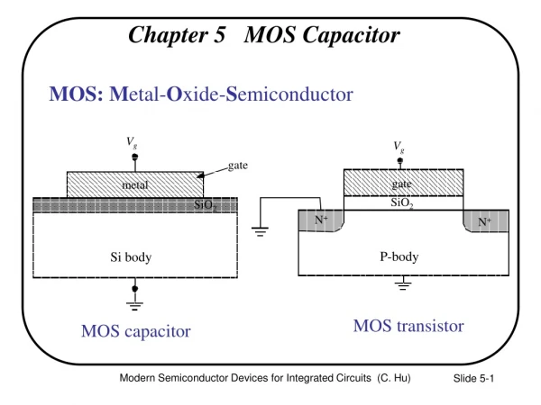
CMOS Inverter Technology • The CMOS inverter consists of a PMOS device stacked on top on an NMOS device, but they need to be fabricated on the same wafer • To accomplish this, the technique of “n-well” implantation is needed as shown in this cross-section of a CMOS inverter Microelectronic Circuit Design, 4E McGraw-Hill
CMOS Inverter • Circuit schematic for a CMOS inverter • Simplified operation model with a high input applied • Simplified operation model with a low input applied Microelectronic Circuit Design, 4E McGraw-Hill
CMOS Inverter Operation • When vI is pulled high (to VDD), the PMOS transistor is turned off, while the NMOS device is turned on pulling the output down to VSS • When vI is pulled low (to VSS), the NMOS transistor is turned off, while the PMOS device is turned on pulling the output up to VDD Microelectronic Circuit Design, 4E McGraw-Hill
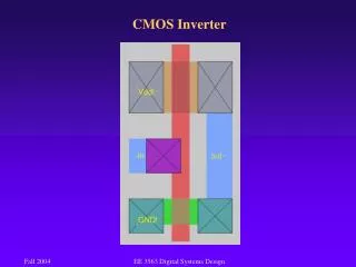
CMOS Inverter Layout • Two methods of laying out a CMOS inverter are shown • The PMOS transistors lie within the n-well, whereas the NMOS transistors lie in the p-substrate • Polysilicon is used to form common gate connections, and metal is used to tie the two drains together Microelectronic Circuit Design, 4E McGraw-Hill
Static Characteristics of the CMOS Inverter • The figure shows the two static states of operation with the circuit and simplified models • Notice that VH = 5V and VL = 0V, and that ID = 0A which means that there is no static power dissipation Microelectronic Circuit Design, 4E McGraw-Hill
CMOS Voltage Transfer Characteristics The VTC shown is for a CMOS inverter that is symmetrical (Kp = Kn). Microelectronic Circuit Design, 4E McGraw-Hill
CMOS Voltage Transfer Characteristics • The simulation results show the varying VTC of the inverter as VDD is changed • The minimum voltage supply for CMOS technology is VDD = 2VT ln(2) V Microelectronic Circuit Design, 4E McGraw-Hill
CMOS Voltage Transfer Characteristics • Simulation results show the varying VTC of the inverter as KN/KP = KR is changed • For KR > 1 the NMOS current drive is greater, and it forces transition region vI < VDD/2 • For KR < 1 the PMOS current drive is greater, and it forces transition region vI > VDD/2 Microelectronic Circuit Design, 4E McGraw-Hill
Noise Margins for the CMOS Inverter Noise margins are defined by the points shown in the given figure Microelectronic Circuit Design, 4E McGraw-Hill
Noise Margins for the CMOS Inverter Microelectronic Circuit Design, 4E McGraw-Hill
Propagation Delay Estimate • The two modes of capacitive charging/discharging that contribute to propagation delay Microelectronic Circuit Design, 4E McGraw-Hill
Propagation Delay Estimate • If it is assumed the inverter in “symmetrical” with (W/L)P = 2.5 (W/L)N, then PLH = PHL Microelectronic Circuit Design, 4E McGraw-Hill
Rise and Fall Times • The rise and fall times are given by the following approximate expressions: Microelectronic Circuit Design, 4E McGraw-Hill
Reference Inverter Design Example • Design a reference inverter to achieve a delay of 250ps with a 0.1pF load given the following information: Microelectronic Circuit Design, 4E McGraw-Hill
Gate Device Geometry Scaling based Upon Reference Circuit Simulation • State-of-the-art short gate length technologies are hard to analyze • Scaling can be used to properly set W/L for a given load capacitance relative to reference gate simulation with a reference load. Scaling allows us to calculate a new geometry (W/L)' in terms of a target load and delay. Jaeger/Blalock 3/15/10 Microelectronic Circuit Design, 4E McGraw-Hill Microelectronic Circuit Design, 4E McGraw-Hill Chap 6 - 18
Performance Scaling • Consider a reference inverter with a delay of 3.16 ns. • What is the delay if an inverter has a W/L 4x larger than the transistors of the reference inverter and twice the load capacitance. Scaling allows us to calculate a new geometry (W/L)' or delay relative to a reference design. Microelectronic Circuit Design, 4E McGraw-Hill
Reference Inverter Design Example • Assuming the inverter is symmetrical and using the values given in Table 7.1: Microelectronic Circuit Design, 4E McGraw-Hill
Reference Inverter Design Example • Solving for RonN: • Then solve for the transistor ratios: Microelectronic Circuit Design, 4E McGraw-Hill
Delay of Cascaded Inverters • An ideal step was used to derive the previous delay equations, but this is not possible to implement • By using putting the following circuit in SPICE, it is possible to produce more accurate equations Microelectronic Circuit Design, 4E McGraw-Hill
Delay of Cascaded Inverters • The simulated output of the previous circuit appears below, and it can be seen that the delay for the nonideal step input is approximately twice than the ideal case: Microelectronic Circuit Design, 4E McGraw-Hill
Static Power Dissipation • CMOS logic is considered to have no static power dissipation • This is not completely accurate since MOS transistors have leakage currents associated with the reverse-biased drain-to-substrate connections as well as sub-threshold leakage current between the drain and source Microelectronic Circuit Design, 4E McGraw-Hill
Dynamic Power Dissipation • There are two components that add to dynamic power dissipation: • Capacitive load charging at a frequency f given by: PD = CV2DDf • The current that occurs during switching which can be seen in the figure Microelectronic Circuit Design, 4E McGraw-Hill
Power-Delay Product • The power-delay product is given as: The figure shows a symmetrical inverter switching waveform Microelectronic Circuit Design, 4E McGraw-Hill
IrDA, Infrared Data Association Audio DAC (Digital to Analog Converter) Microelectronic Circuit Design, 4E McGraw-Hill
CMOS NOR Gate Basic CMOS logic gate structure CMOS NOR gate implementation Reference Inverter Microelectronic Circuit Design, 4E McGraw-Hill
CMOS NOR Gate Transistor Sizing • When sizing the transistors, we attempt to keep the delay times the same as the reference inverter • To accomplish this, the on-resistance in the PMOS and NMOS branches of the NOR gate must be the same as the reference inverter • For a two-input NOR gate, the (W/L)p must be made twice as large Microelectronic Circuit Design, 4E McGraw-Hill
CMOS NOR Gate Body Effect • Since the bottom PMOS body contact is not connected to its source, its threshold voltage changes as VSBchanges during switching • Once vO = VH is reached, the bottom PMOS is not affected by body effect, thus the total on-resistance of the PMOS branch is the same • However, the rise time is slowed down slightly due to |VTP| being a function of time Microelectronic Circuit Design, 4E McGraw-Hill
Two-Input NOR Gate Layout Microelectronic Circuit Design, 4E McGraw-Hill
Three-Input NOR Gate Layout • It is possible to extend this same design technique to create multiple input NOR gates Microelectronic Circuit Design, 4E McGraw-Hill
Shorthand Notation for NMOS and PMOS Transistors Microelectronic Circuit Design, 4E McGraw-Hill
CMOS NAND Gates CMOS NAND gate implementation Reference Inverter Microelectronic Circuit Design, 4E McGraw-Hill
CMOS NAND Gate Transistor Sizing • The same rules apply for sizing the NAND gate devices as for the NOR gate, except now the NMOS transistors are in series • (W/L)N will be twice the size of that of the reference inverter Microelectronic Circuit Design, 4E McGraw-Hill
Multi-Input CMOS NAND Gates Microelectronic Circuit Design, 4E McGraw-Hill
Complex CMOS Logic GateDesign Example – Euler path • Design a CMOS logic gate for (W/L)p,ref = 5/1 and for (W/L)n,ref = 2/1 that yields the function: Y = A + BC +BD • By inspection (knowing Y), the NMOS branch of the gate can drawn as the following with the corresponding graph, while considering the longest path for sizing purposes: Microelectronic Circuit Design, 4E McGraw-Hill
Complex CMOS Logic Gate Design Example • By placing nodes in the interior of each arc, plus two more outside the graph for VDD (3) and the complementary output (2’), the PMOS branch can be realized as shown on the left figure • Connect all of the nodes in the manner shown in the right figure, and the NMOS arc’s that the PMOS arc’s intersect have the same inputs Microelectronic Circuit Design, 4E McGraw-Hill
Complex CMOS Logic Gate Design Example • From the PMOS graph, the PMOS network can now be drawn for the final CMOS logic gate while once again considering the longest PMOS path for sizing Two equivalent forms of the final circuit Microelectronic Circuit Design, 4E McGraw-Hill
Complex CMOS Gate with a Bridging Transistor - Design Example • Design a CMOS gate that implements the following logic function using the same reference inverter sizes as the previous example: Y = AB +CE + ADE + CDB • The NMOS branch can be realized in the following manner using bridging NMOS D to implement Y. The corresponding NMOS graph is shown to the right. Microelectronic Circuit Design, 4E McGraw-Hill
Complex CMOS Gate with a Bridging Transistor - Design Example • By using the same technique as before, the PMOS graph can now be drawn Microelectronic Circuit Design, 4E McGraw-Hill
Complex CMOS Gate with a Bridging Transistor - Design Example • By using the PMOS graph, the PMOS network can now be realized as shown (considering the longest path for sizing) Microelectronic Circuit Design, 4E McGraw-Hill
Minimum Size Gate Design and Performance • With CMOS technology, there is an area/delay tradeoff that needs to be considered • If minimum feature sized are used for both devices, then the PLHwill be increased compared to the symmetrical reference inverter Microelectronic Circuit Design, 4E McGraw-Hill
Minimum Size Complex Gate and Layout • The following shows the layout of a complex minimum size logic gate Microelectronic Circuit Design, 4E McGraw-Hill
Minimum Size Complex Gate and Layout Microelectronic Circuit Design, 4E McGraw-Hill
Dynamic Domino CMOS Logic • One technique to help decrease power in MOS logic circuits is dynamic logic • Dynamic logic uses different precharge and evaluation phases that are controlled by a system clock to eliminate the dc current path in single channel logic circuits • Early MOS logic required multiphase clocks to accomplish this, but CMOS logic can be operated dynamically with a single clock Microelectronic Circuit Design, 4E McGraw-Hill

