Download
1 / 42
500 likes | 1.21k Vues
This chapter delves into the fundamental concepts of Metal-Oxide-Semiconductor (MOS) capacitors, essential components in modern integrated circuits. It covers the flat-band condition, surface accumulation, depletion, and threshold voltages, providing detailed energy band diagrams and equations governing the behavior of these devices under varying gate voltages. The MOS capacitor's role in controlling the charge in semiconductor devices is emphasized, presenting key parameters like capacitance-voltage characteristics while enhancing comprehension of MOS technology's application in integrated circuits.

E N D
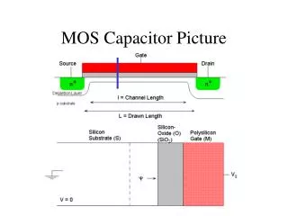
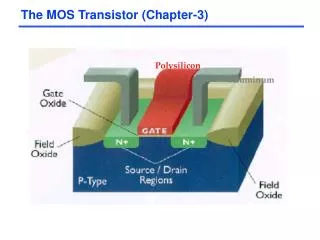
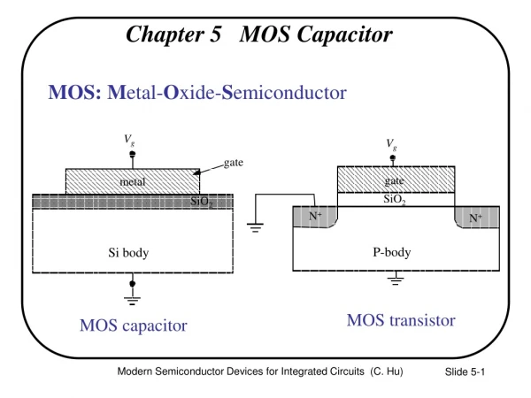
Chapter 5 MOS Capacitor MOS: Metal-Oxide-Semiconductor Vg Vg gate gate metal SiO2 SiO2 N+ N+ P-body Si body MOS transistor MOS capacitor Modern Semiconductor Devices for Integrated Circuits (C. Hu)
Ec Ec Ef , Ec Ef Ev Ev Gate Si Body Ev Chapter 5 MOS Capacitor n y o d c o i l b i s 2 O y n l i o S o c p i l i + S N - P This energy-band diagram for Vg = 0 is not the simplest one. Modern Semiconductor Devices for Integrated Circuits (C. Hu)
5.1 Flat-band Condition and Flat-band Voltage E 0 =0.95 eV c SiO 2 E c y q y = + ( – ) g c q E E c 3.1 eV 3.1 eV s Si c f Si =4.05eV E E E c , f c V q fb E f E E v v 9 eV P-body N + -poly-Si The band is flat at theflat band voltage. E0 : Vacuum level E0 – Ef : Work function E0 –Ec : Electron affinity Si/SiO2 energy barrier 4.8 eV E v SiO 2 Modern Semiconductor Devices for Integrated Circuits (C. Hu)
3.1eV V ox E E is negligible when c , f E E v 0 qV g f q E s c the surface is in accumulation. E f E v M O S 5.2 Surface Accumulation Make Vg < Vfb fs : surface potential, band bending Vox: voltage across the oxide Modern Semiconductor Devices for Integrated Circuits (C. Hu)
Gauss’s Law 5.2 Surface Accumulation Vg <Vt Modern Semiconductor Devices for Integrated Circuits (C. Hu)
5.3 Surface Depletion ( ) V > V g fb qV ox E c f q s gate E - + + + + + + f - - E - SiO v qV 2 - - - - - - - g - - - - - - - W - - - - - - - E E dep V c , f depletion layer depletion charge, Q region dep E v P-Si body M O S Modern Semiconductor Devices for Integrated Circuits (C. Hu)
5.3 Surface Depletion This equation can be solved to yield fs . Modern Semiconductor Devices for Integrated Circuits (C. Hu)
E c f st E i = f q A C B E f D B E = qV qV v g t E E c , f E v M O S 5.4 Threshold Condition and Threshold Voltage Threshold (of inversion): ns = Na, or (Ec–Ef)surface= (Ef –Ev)bulk , or A=B, and C = D Modern Semiconductor Devices for Integrated Circuits (C. Hu)
= + + V V φ V g fb s ox Threshold Voltage At threshold, Modern Semiconductor Devices for Integrated Circuits (C. Hu)
+ for P-body, – for N-body Threshold Voltage Modern Semiconductor Devices for Integrated Circuits (C. Hu)
> V V g t E c - E gate f - - E - v ++++++++++ - - SiO 2 qV g - - - - - - - - - - - - - - - V E E c , f Q Q dep inv E - Si substrate P v M O S 5.5 Strong Inversion–Beyond Threshold Vg > Vt Modern Semiconductor Devices for Integrated Circuits (C. Hu)
Inversion Layer Charge, Qinv (C/cm2) Vg > Vt Vg > Vt Modern Semiconductor Devices for Integrated Circuits (C. Hu)
5.5.1 Choice of Vt and Gate Doping Type Vt is generally set at a small positive value so that, at Vg = 0, the transistor does not have an inversion layer and current does not flow between the two N+ regions • P-body is normally paired with N+-gate to achieve a small positive threshold voltage. • N-body is normally paired with P+-gate to achieve a small negative threshold voltage. Modern Semiconductor Devices for Integrated Circuits (C. Hu)
Review : Basic MOS Capacitor Theory fs 2fB Vg Vt Vfb accumulation depletion inversion Wdep W dmax 1/2 W = (2 e 2 f / q N ) B dmax s a µ f ( ) 1/2 s Vg Vfb Vt accumulation depletion inversion Modern Semiconductor Devices for Integrated Circuits (C. Hu)
Review : Basic MOS Capacitor Theory Qdep=- qNaWdep total substrate charge, Qs Vfb accumulation depletion inversion Vg (a) 0 Vt –qNaWdep –qNaWdmax Qinv Qs inversion depletion accumulation accumulation depletion inversion regime regime regime Vg (b) Vfb Vt slope = -Cox Vfb Vg 0 Vt Qacc Qinv slope = -Cox (c) slope = -Cox Vfb Vt Vg accumulation depletion inversion Modern Semiconductor Devices for Integrated Circuits (C. Hu)
MOS Capacitor C-V Meter 5.6 MOS CV Characteristics Modern Semiconductor Devices for Integrated Circuits (C. Hu)
5.6 MOS CV Characteristics Qs accumulation depletion inversion C regime regime regime Cox Vfb Vg 0 Vt Qinv Vg slope = -Cox Vfb Vt accumulation depletion inversion Modern Semiconductor Devices for Integrated Circuits (C. Hu)
C Cox Vg Vfb Vt accumulation depletion inversion CV Characteristics In the depletion regime: Modern Semiconductor Devices for Integrated Circuits (C. Hu)
gate gate C C ox ox + + + + + + + + + C dep - - - - - - P-substrate P-substrate gate C ox DC - - - - - - - - - C - - - - dmax - AC W dmax P-substrate Supply of Inversion Charge May be Limited Wdep Accumulation Depletion gate C ox - - - - - - - - N + Inversion Inversion Wdmax DC and AC P-substrate In each case, C = ? Modern Semiconductor Devices for Integrated Circuits (C. Hu)
Capacitor and Transistor CV (or HF and LF CV) Modern Semiconductor Devices for Integrated Circuits (C. Hu)
C Cox Vg Vfb Vt accumulation depletion inversion Quasi-Static CV of MOS Capacitor The quasi-static CV is obtained by the application of a slow linear-ramp voltage (< 0.1V/s) to the gate, while measuring Ig with a very sensitive DC ammeter. C is calculated from Ig = C·dVg/dt. This allows sufficient time for Qinv to respond to the slow-changing Vg. Modern Semiconductor Devices for Integrated Circuits (C. Hu)
MOS transistor CV, C QS CV HF capacitor CV Vg EXAMPLE : CV of MOS Capacitor and Transistor Does the QS CV or the HF capacitor CV apply? (1) MOS transistor, 10kHz. (Answer: QS CV). (2) MOS transistor, 100MHz. (Answer: QS CV). (3) MOS capacitor, 100MHz. (Answer: HF capacitor CV). (4) MOS capacitor, 10kHz. (Answer: HF capacitor CV). (5) MOS capacitor, slow Vg ramp. (Answer: QS CV). (6) MOS transistor, slow Vg ramp. (Answer: QS CV). Modern Semiconductor Devices for Integrated Circuits (C. Hu)
5.7 Oxide Charge–A Modification to Vfb and Vt Modern Semiconductor Devices for Integrated Circuits (C. Hu)
5.7 Oxide Charge–A Modification to Vfb and Vt Types of oxide charge: • Fixed oxide charge, Si+ • Mobile oxide charge, due to Na+contamination • Interface traps, neutral or charged depending on Vg. • Voltage/temperature stress induced charge and traps--a reliability issue Modern Semiconductor Devices for Integrated Circuits (C. Hu)
Vfb 10 nm 20 nm 30 nm Tox 0 –0.15V –0.3V EXAMPLE: Interpret this measured Vfbdependence on oxide thickness. The gate electrode is N+ poly-silicon. What does it tell us? Body work function? Doping type? Other? Solution: Modern Semiconductor Devices for Integrated Circuits (C. Hu)
from intercept E , vacuum level 0 y y = y + 0.15V g s g E , E E f c c E f E E v v + N -Si gate Si body N-type substrate, from slope Modern Semiconductor Devices for Integrated Circuits (C. Hu)
= e W / qN E dpoly ox ox poly P+ 5.8 Poly-Silicon Gate Depletion–Effective Increase in Tox Gauss’s Law If Wdpoly= 15 Å, what is the effective increase in Tox? Modern Semiconductor Devices for Integrated Circuits (C. Hu)
Effect of Poly-Gate Depletion on Qinv • Poly-gate depletion degrades MOSFET current and circuit speed. W dpoly E c • How can poly-depletion be minimized? E , E f v q f poly E c E f E v + P -gate N-substrate Modern Semiconductor Devices for Integrated Circuits (C. Hu)
= e = e W / qN V / T qN E dpoly ox ox poly ox ox ox poly - 14 3 . 9 8 . 85 10 ( F/cm ) 1 V = - - - 7 19 19 3 2 10 cm 1 . 6 10 C 8 10 cm = 1 . 3 nm EXAMPLE : Poly-Silicon Gate Depletion Vox , the voltage across a 2 nm thin oxide, is –1 V. The P+poly-gate doping is Npoly = 8 1019 cm-3 and substrate Nd is 1017cm-3. Find (a) Wdpoly , (b) fpoly , and (c) Vg . Solution: (a) Modern Semiconductor Devices for Integrated Circuits (C. Hu)
EXAMPLE : Poly-Silicon Gate Depletion (b) (c) Is the loss of 0.11 V from the 1.01 V significant? Modern Semiconductor Devices for Integrated Circuits (C. Hu)
Tinv Si Gate A -50 -40 -30 -20 -10 0 10 20 30 40 50 Physical T ox Effective T ox 5.9 Inversion and Accumulation Charge-Layer Thickness–Quantum Mechanical Effect Average inversion-layer location below the Si/SiO2 interface is called the inversion-layer thickness, Tinv. n(x) is determined by Schrodinger’s eq., Poisson eq., and Fermi function. Modern Semiconductor Devices for Integrated Circuits (C. Hu)
at Vg=Vdd Electrical Oxide Thickness, Toxe • Tinv is a function of the average electric field in the inversion layer, which is (Vg+ Vt)/6Tox (Sec. 6.3.1). • Tinv of holes is larger than that of electrons because of difference in effective mass. • Toxe is the electrical oxide thickness. Modern Semiconductor Devices for Integrated Circuits (C. Hu)
= + + T T W / 3 T / 3 oxe ox dpoly inv Effective Oxide Thickness and Effective Oxide Capacitance C Basic CV C ox with poly-depletion with poly-depletion and charge-layer thickness measured data Vg Modern Semiconductor Devices for Integrated Circuits (C. Hu)
Equivalent circuit in the depletion and the inversion regimes (d) (a) (c) (b) General case for both depletion and inversion regions. In the depletion regions VgVt Strong inversion Modern Semiconductor Devices for Integrated Circuits (C. Hu) Slide 5-34
5.10 CCD Imager and CMOS Imager 5.10.1 CCD Imager Deep depletion, Qinv= 0 Exposed to light Modern Semiconductor Devices for Integrated Circuits (C. Hu)
V3 V2 V1 V1 > V2 = V3 oxide - - - - - - - - - - - - - (a) depletion region - - P-Si V3 V3 V2 V1 V1 V1 V2 V2 > V1 > V3 oxide - - - - - - - - depletion region (b) P-Si V2 V2 V1 V3 V1 V3 V1 V2 > V1 = V3 oxide - - - - - - - - depletion region (c) P-Si CCD Charge Transfer Modern Semiconductor Devices for Integrated Circuits (C. Hu)
two-dimensional CCD imager Signal out Reading row, shielded from light Charge-to-voltage converter The reading row is shielded from the light by a metal film. The 2-D charge packets are read row by row. Modern Semiconductor Devices for Integrated Circuits (C. Hu) Slide 5-37
PN junction charge collector switch V1 Amplifier circuit V2 V3 Signal out Shifter circuit 5.10.2 CMOS Imager CMOS imagers can be integrated with signal processing and control circuitries to further reduce system costs. However, The size constrain of the sensing circuits forces the CMOS imager to use very simple circuits Modern Semiconductor Devices for Integrated Circuits (C. Hu) Slide 5-38
5.11 Chapter Summary N-type device: N+-polysilicon gate over P-body P-type device: P+-polysilicon gate over N-body Modern Semiconductor Devices for Integrated Circuits (C. Hu)
or 5.11 Chapter Summary + : N-type device, – : P-type device Modern Semiconductor Devices for Integrated Circuits (C. Hu)
5.11 Chapter Summary N-type Device (N+-gate over P-substrate) P-type Device (P+-gate over N-substrate) What’s the diagram like at Vg > Vt? at Vg= 0? Modern Semiconductor Devices for Integrated Circuits (C. Hu)
5.11 Chapter Summary What is the root cause of the low C in the HF CV branch? Modern Semiconductor Devices for Integrated Circuits (C. Hu)