The MOS Transistor (Chapter-3)
690 likes | 1k Vues
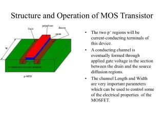
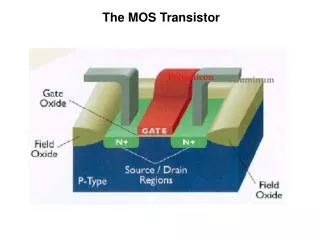
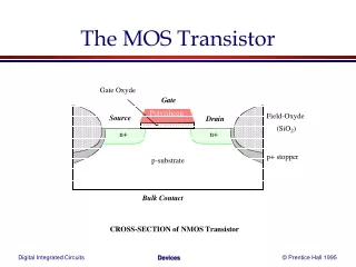
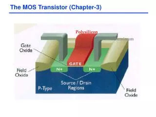
The MOS Transistor (Chapter-3). Polysilicon. Aluminum. n areas have been doped with donor ions (arsenic) of concentration N D - electrons are the majority carriers. L. Gate oxide. Polysilicon Gate. W. Source. Drain. Field-Oxide (SiO 2 ). n+. n+. p substrate. p+ stopper.

The MOS Transistor (Chapter-3)
E N D
Presentation Transcript
The MOS Transistor (Chapter-3) Polysilicon Aluminum
n areas have been doped with donor ions (arsenic) of concentration ND - electrons are the majority carriers L Gate oxide Polysilicon Gate W Source Drain Field-Oxide (SiO2) n+ n+ p substrate p+ stopper Bulk (Body) p areas have been doped with acceptor ions (boron) of concentration NA - holes are the majority carriers The NMOS Transistor Cross Section
Closed (on) (Gate = ‘1’) Open (off) (Gate = ‘0’) Ron Switch Model of NMOS Transistor Gate | VGS | Source (of carriers) Drain (of carriers) | VGS | < | VT | | VGS | > | VT |
Closed (on) (Gate = ‘0’) Open (off) (Gate = ‘1’) Ron Switch Model of PMOS Transistor Gate | VGS | Source (of carriers) Drain (of carriers) | VGS | > | VDD – | VT | | | VGS | < | VDD – |VT| |
VGS + - n+ depletion region n channel Threshold Voltage Concept G D S n+ p substrate B The value of VGS where strong inversion occurs is called the threshold voltage, VT
MOS gate Structure • First electrode - Gate : Consists of low-resistivity material such as highly-doped polycrystalline silicon, aluminum or tungsten • Second electrode - Substrate or Body: n- or p-type semiconductor • Dielectric - Silicon dioxide: stable high-quality electrical insulator between gate and substrate.
Gate and Substrate Conditions for Different Biases Accumulation VG << VTN Depletion VG < VTN Inversion VG > VTN
The Threshold Voltage VT = VT0 + (|-2F + VSB| - |-2F|) where VT0 is the threshold voltage at VSB = 0 and is mostly a function of the manufacturing process • Difference in work-function between gate and substrate material, oxide thickness, Fermi voltage, charge of impurities trapped at the surface, dosage of implanted ions, etc. VSB is the substrate-bias voltage F = -Tln(NA/ni) is the Fermi potential (T = kT/q = 26mV at 300K is the thermal voltage; NA is the acceptor ion concentration; ni 1.5x1010 cm-3 at 300K is the intrinsic carrier concentration in pure silicon) = (2qsiNA)/Coxis the body-effect coefficient (impact of changes in VSB) (si=1.053x10⁻¹⁰F/m is the permittivity of silicon; Cox = ox/tox is the gate oxide capacitance with ox=3.5x10⁻¹¹F/m)
The Body Effect • VSB is the substrate bias voltage (normally positive for n-channel devices with the body tied to ground) • A negative bias causes VT to increase from 0.45V to 0.85V VT (V) VBS (V)
- + V(x) ID n+ x Transistor in Linear Mode Assuming VGS > VT VGS VDS G S D n+ B The current is a linear function of both VGS and VDS
MOSFET Current –Voltage Characteristics (Linear region) • The applied gate voltage needed to create an inversion charge layer in the semiconductor substrate is called threshold voltage (VTN orVt). • At Vt the charge density is equal to the concentration of majority carriers in the semiconductors substrate.
Concept of Asymmetric Channel • It is to be noted that the VDS measured relative to the source increases from 0 to VDS as we travel along the channel from source to drain. This is because the voltage between the gate and points along the channel decreases from VGS at the source end to VGS-VDS. • When VDS is increased to the value that reduces the voltage between the gate and channel at the drain end to Vt that is , • VGS-VDS=Vt or VDS= VGS-Vt or VDS(sat) ≥ VGS-Vt
MOSFET Current –Voltage Characteristics (Saturation Region) • When VDS is increased to the value that reduces the voltage between the gate and channel at the drain end to Vt that is , VGS-VDS=Vt or VDS= VGS-Vt At this point the channel depth at the drain end decreases to almost zero, and the channel is said to be pinched off. Increasing VDS beyond this value has no effect on the channel shape. The MOSFET is said to have entered the saturation region, the drain current is essentially independent of VDS for constant VGS. VDSsat= VGS-Vt Obviously, for every value of VGS≥Vt, there is a corresponding value of VDSsat
ID n+ n+ Pinch-off - + VGS - VT Transistor in Saturation Mode Assuming VGS > VT VDS > VGS - VT VGS VDS G S D B The current remains constant (saturates).
NMOS Transistor: Saturation Region is called the saturation or pinch-off voltage
MOSFET Current –Voltage Relationships (Non saturation Region) • The region for which VDS< VDS(sat) is known as the nonsaturation region. The ideal current voltage characteristics in this region are describe by the equation iD= Kn[(VGS-VTN)VDS-VDS2/2] Where the parameter Kn is called the conduction parameter or gain factor for the n-channel device and is given by Kn= nCoxW/L Where Cox is the oxide capacitance per unit area. The capacitance is given by Cox= ox/tox Where tox is the oxide thickness and ox is the oxide permittivity. The parameter n is the mobility of the electron in the inversion layer.
MOSFET Current –Voltage Relationships (Saturation Mode) • In saturation mode VDS ≥ VGS-Vt . The expression for saturation mode can be obtained by substituting VDS = VGS-Vt resulting in iD (Sat)= Kn/2(VGS-VTN)2 This expression indicates that the saturation drain current has no dependence on VDS.
Process Tranconductance parameter • It is to be noted that in the above expressions the parameter nCox is a constant determined by the processing technology used to fabricate the MOS technology. It is known as the process transconductance parameter, and is denoted by K'n= nCox • We can rewrite the conduction parameter in the form, Kn= K'nW/L Transistor design variable.
Channel-Length Modulation • As vDS increases abovevDSAT, thelength of the depleted channel beyond pinch-off point, DL, increases and actual L decreases. • iD increases slightly with vDSinstead of being constant. l = channel length modulation parameter
Current Determinates • For a fixed VDS and VGS (> VT), IDS is a function of • the distance between the source and drain – L • the channel width – W • the threshold voltage – VT • the thickness of the SiO2 – tox • the dielectric of the gate insulator (SiO2) – ox • the carrier mobility • for n: n = 500 cm2/ V-sec • for p: p = 180 cm2/ V-sec iD= Kn[(VGS-VTN)VDS-VDS2/2]
p-Channel MOSFET • In p-channel enhancement device. A negative gate-to-source voltage must be applied to create the inversion layer, or channel region, of holes that, “connect” the source and drain regions. • The threshold voltage VTP for p-channel enhancement load device is always negative and positivefor depletion-mode PMOS. • Cross-section of p-channel enhancement mode MOSFET The operation of the p-channel is same as the n-channel device , except that the hole is the charge carrier, rather than the electron, and the conventional current direction and voltage polarities are reversed.
Summary of the MOSFET Current-Voltage relationship Table 5.1
Example • Given that for n-channel enhancement mode MOSFET, VTN=1.2V and VGS=2V Determine the region of the operation when: • VDS=0.4V • VDS= 1V • VDS=5V Sol: We know at the saturation, VDS(sat)=VGS-VTN= 2-1.2=0.8V Case1: when VDS=0.4V • VDS < VDS(sat) transistor is in nonsaturation region CaseII: when VDS=1V VDS > VDS(sat) transistor is in saturation mode CaseIII: when VDS=5V • VDS > VDS (sat) transistor is in saturation mode
Secondary effects • Short-channel effects: • Short channel device has channel length comparable to depth of drain and source junctions and depletion width • Causes threshold voltage and I/V curve variations • Narrow-channel effects: • Narrow channel device has small channel width • Subthreshold conduction (leakage current)
Short-channel effects • Short-channel device: channel length is comparable to depth of drain and source junctions and depletion width • In general, visible when L ~ 1m and below • Short-channeleffects: • Carrier velocity saturation • Mobility degradation • Threshold voltage variation
Carrier velocity saturation Vgs 0 Vds • Electric field Ey exists along channel • As channel length is reduced, electric field increases (if voltage is constant) • Electron drift velocity vd is proportional to electric field • only for small field values • for large electric field, velocity saturates N+ N+ source drain L P
Effects of High fields • Vertical field The vertical field occurs in the y-direction from the gate to the channel (EY=VDD/tox 1980 1995 2001 EY=5V/1000Ao =50 x 104V/cm EY=3.3.V/75Ao=4.4 x 106V/cm Ey=1.2V/22AO=5.5 x 106 V/cm • Horizontal field The horizontal field occurs in the x-direction from the drain to the source (EY=VDS/L 1980 1995 2001 Ex=5V/5mm =104V/cm Ex=3.3.V/0.35mm=9.4 x 104V/cm Ex=1.2V/0.1mm=1.2 x 105 V/cm
Carrier velocity saturation • Effect of velocity saturation: • Current saturates before “saturation region” • VDSAT = voltage at which saturation occurs • Drain current is reduced: (no longer quadratic function of VGS) • Saturation region is extended: VDSAT < VGS-VT
VGS = VDD Velocity Saturation Effects For short channel devices and large enough VGS – VT Long channel devices • VDSAT < VGS – VT so the device enters saturation before VDS reaches VGS – VT and operates more often in saturation Short channel devices VDSAT VGS-VT • IDSAT has a linear dependence wrt VGS so a reduced amount of current is delivered for a given control voltage
Linear dependence Linear Saturation Short Channel I-V Plot (NMOS) X 10-4 Early Velocity Saturation VGS = 2.5V VGS = 2.0V ID (A) VGS = 1.5V VGS = 1.0V VDS (V) NMOS transistor, 0.25m, Ld = 0.25m, W/L = 1.5, VDD = 2.5V, VT = 0.4V
MOS ID-VGS Characteristics • Linear (short-channel) versus quadratic (long-channel) dependence of ID on VGS in saturation • Velocity-saturation causes the short-channel device to saturate at substantially smaller values of VDS resulting in a substantial drop in current drive X 10-4 long-channel quadratic ID (A) short-channel linear VGS (V) (for VDS = 2.5V, W/L = 1.5)
Short-channel and long channel comparison Long-channel Short-channel • Both devices have same effective W/L ratio I/V curves should be similar • Short-channel device has ~ 40% less current at high VDS • Note linear dependence on VGS in short-channel device
Mobility degradation • MOS I/V equations depend on surface mobility mn (or mp) • In short-channel devices, mn and mp are not constant • As vertical electric field EY increases, surface mobility decreases • 0 = low-field mobility, is empirical constant • As VGS increases, surface mobility decreases
Threshold voltage variation • Until now, threshold voltage assumed constant • VT changed only by substrate bias VSB • In threshold voltage equations, channel depletion region assumed to be created by gate voltage only • Depletion regions around source and drain neglected: valid if channel length is much larger than depletion region depths • In short-channel devices, depletion regions from drain and source extend into channel
Threshold voltage variation Short-channel effects cause threshold voltage variation: • VT roll off • As channel length L decreases, threshold voltage decreases • Drain-induced barrier lowering • As drain voltage VDS increases, threshold voltage decreases • Hot-carrier effect • Threshold voltages drift over time
Threshold voltage variation • Even with VGS=0, part of channel is already depleted • Bulk depletion charge is smaller in short-channel device → VT is smaller N+ source N+ drain Drain depletion region Source depletion region Gate-induced depletion region
Threshold voltage variation • Change in VT0: • xdS, xdD: depth of depletion regions at S, D • xj: junction depth • VT0 is proportional to (xj/L) • For short channel lengths, VT0 is large • For large channel lengths, term approaches 0
Threshold voltage variations Graphically: VT0 versus channel length L Threshold as a function of As a function of length (for low VDS) Drain-induced barrier lowering (for low L) VT Roll-off:VT decreases rapidly with channel length
Drain-induced barrier lowering (DIBL) • Drain-induced barrier lowering (DIBL) • Drain voltage VDS causes change in threshold voltage • As VDS is increased, threshold voltage decreases • Cause: depletion region around drain • Depletion region depth around drain depends on drain voltage • As VDS is increased, drain depletion region gets deeper and extends further into channel • For very large VDS, source and drain depletion regions can meet → punch-through! • Issue: results in uncertainty in circuit design
Threshold voltage variation • Hot-carrier effect • increased electric fields causes increased electron velocity • high-energy electrons can tunnel into gate oxide • This changes the threshold voltage (increases VT for NMOS) • Can lead to long-term reliability problems
Threshold voltage variation • Hot electrons • High-velocity electrons can also impact the drain, dislodging holes • Holes are swept towards negatively-charged substrate → cause substrate current- • Called impact ionization • This is another factor which limits the process scaling → voltage must scale down as length scales