Download
1 / 62
680 likes | 1.11k Vues
Chapter 2 MOS Transistor Theory. Boonchuay Supmonchai Integrated Design Application Research ( IDAR ) Laboratory June 16th, 2004; Revised June 16th, 2005. Goal of this chapter. Present intuitive understanding of device operation Introduction of device basic equations

E N D
Chapter 2MOS Transistor Theory Boonchuay Supmonchai Integrated Design Application Research (IDAR) Laboratory June 16th, 2004; Revised June 16th, 2005
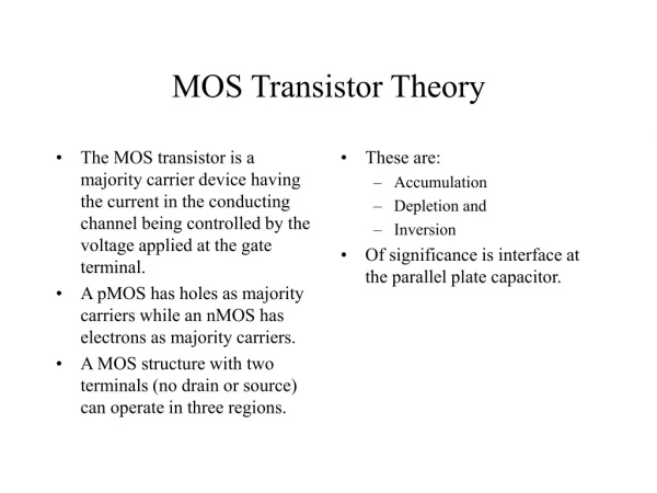
Goal of this chapter • Present intuitive understanding of device operation • Introduction of device basic equations • Introduction of models for manual analysis • First-Order Model • Analysis of secondary and deep-sub-micron effects • Future trends MOS Transistor Theory
B A Al SiO 2 p n Cross-section of pn -junction in an IC process A Al A p n B B One-dimensional representation diode symbol The Diode Mostly occurring as parasitic element in Digital ICs MOS Transistor Theory
Diode - Depletion Region MOS Transistor Theory
Diode - Zero Bias • Build-in (Electrostatic) Potential: T = Thermal Voltage = kt/q = 26 mV at 300 K (Si) ni= Intrinsic carrier concentration ~ 1.5 x 1010 cm-3 NA = Acceptor concentration (atoms/cm3) ND = Donor concentration (atoms/cm3) MOS Transistor Theory
Excess Carriers Excess Carriers Diffusion Diffusion Diode - Forward Bias current Typically avoided in Digital ICs MOS Transistor Theory
Diffusion Diffusion Diode - Reverse Bias current The Dominant Operation Mode MOS Transistor Theory
0.37pn0 Linear Approximation Exponentially Distributed Diode Types Short-Base Diode is the standard in semiconductor devices MOS Transistor Theory
Diode Current VD = Diode Bias Voltage, ID = Diode Current MOS Transistor Theory
(typ. 0.7 V) First-order Diode Model Ideal Diode Model Models for Diode Manual Analysis Is = Saturation Current ~ 10-17 A/m2 MOS Transistor Theory
Graphic Solution ID = 0.224 mA VD= 0.757 V Example: A Diode Circuit 1: ID = IS [exp(VD /T) - 1] 2: ID = (VS - VD)/RS • Using VD(ON) = 0.7 V • ID = 0.23 mA • VD= 0.7 V MOS Transistor Theory
Diode - Junction Capacitance Cj0 = Zero-Biased Junction Capacitance = f(physical parameters) m = Grading Coefficient (0.5 - Abrupt, 0.33 - linear ) MOS Transistor Theory
Diode - Diffusion Capacitance = mean transit time = average time for a carrier to be transported from the junction to the metallic contact MOS Transistor Theory
R src V D V 1 I D V src V 2 t = 0 t = T Excess charge Space charge D V OFF ON ON Time Diode Switching Time Switching Time is strongly determined by how fast the charge can be moved around MOS Transistor Theory
Ecrit= 2x10⁵ V/cm -20 Breakdown Voltage Diode - Secondary Effects I Avalanche Breakdown At Critical Field Ecrit, carriers crossing the depletion region is accelerated to high velocity such that when they collide with immobile silicon atoms, electron-hole pairs are created MOS Transistor Theory
ID increases 6% per ºC (2X every 12 º C) Diode - Secondary Effects II Temperature Effects IS = f(T) Theory: 2X every 5ºC Experiment: 2X every 8ºC T T (For fixed ID) VD decreases 2mV per ºC MOS Transistor Theory
Neutral Regions + VD - ID Diode SPICE Model n = emission coefficient (≥ 1) MOS Transistor Theory
SPICE Diode Model Parameters MOS Transistor Theory
What is a MOS(FET) Transistor? • Metal-Oxide-Semiconductor Field-Effect Transistor (MOSFET, or MOS, for short) • A Four-terminal device • Gate controls how much current can flow from the Source to the Drain. • Body modulates device characteristics and parameters - secondary effect. • A switch! MOS Transistor Theory
D D G G S S NMOS Enhancement NMOS Depletion D D G B G S S PMOS Enhancement NMOS with Bulk Contact MOS Transistors - Types and Symbols The Body terminal, if not shown, is assumed to be connected to the appropriate supply. MOS Transistor Theory
Gate | VGS | Source (of carriers) Drain (of carriers) Closed (on)(Gate = ‘1’) Open (off)(Gate = ‘0’) Ron Switch Model of NMOS Transistor | VGS | > | VT | | VGS | < | VT | MOS Transistor Theory
Gate | VGS | Source (of carriers) Drain (of carriers) Closed (on)(Gate = ‘1’) Open (off)(Gate = ‘0’) Ron Switch Model of PMOS Transistor | VGS | < | VDD – |VT| | | VGS | > | VDD – | VT | | MOS Transistor Theory
Why MOS Transistor? • MOS performs well as a switch with very few parasitic effects. • Relatively “Simple” manufacturing process (compared to other types of transistor) • High Integration Density • Large and Complex circuits can be created economically. MOS Transistor Theory
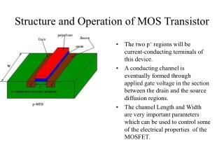
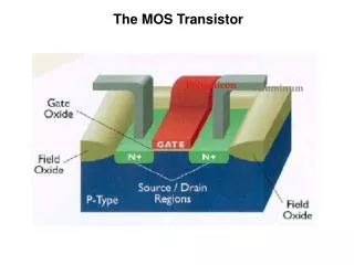
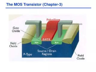
Polysilicon Aluminum The NMOS Transistor MOS Transistor Theory
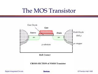
L Gate oxide Polysilicon Gate W Source Drain Field-Oxide (SiO2) n+ n+ p substrate p+ stopper Bulk (Body) The NMOS Transistor Cross Section • nareas have been doped withdonorions (arsenic) of concentration ND - electrons are the majority carriers • pareas have been doped withacceptorions (boron) of concentration NA - holes are the majority carriers MOS Transistor Theory
MOS Transistors - Behaviors • Static Behavior: • Threshold Voltage • Channel-Length Modulation • Velocity Saturation • Sub-threshold Conduction • Dynamic (Transient) Behavior: • MOS Structure Capacitances • Channel Capacitances • Junction Capacitances • Sources-Drain Parasitic Resistance MOS Transistor Theory
G VGS + D S n+ n+ n+ n+ n channel depletion region p substrate p substrate B Threshold Voltage Concept The value of VGS where strong inversion occurs is called thethreshold voltage, VT MOS Transistor Theory
Threshold Voltage Components I • Work function difference between the gate and the channel, GC • GC = F(substrate) - M for metal gate • GC = F(substrate) - F(gate) for polysilicon gate • Gate voltage component to change (invert) the surface potential, 2F • Fermi Potential, F = T ln(NA / ni) • F ~ -0.3 V for p-type silicon substrate MOS Transistor Theory
Threshold Voltage Components II • Gate voltage component to offset the depletion region charge, QB / Cox • Gate Oxide Capacitance per unit area, Cox = ox / tox • Depletion region charge, • Voltage component to offset fixed charges in the gate oxide and in the silicon-oxide surface, QS / Cox • Threshold adjustment by applying the ion implant-ation into the channel, QI / Cox MOS Transistor Theory
The Threshold Voltage Body-effect coefficient MOS Transistor Theory
VSBnormally positive for n-channel devices with the body tied to ground A negative bias causes VT to increase from 0.45V to 0.85V 0.9 0.85 0.8 0.75 0.7 0.65 VT (V) 0.6 0.55 0.5 0.45 0.4 -2.5 -2 -1.5 -1 -0.5 0 VSB (V) The Body Effect - Empirically MOS Transistor Theory
VGS VDS G S n+ D ID n+ n+ n+ x B - + V(x) Transistor in Resistive (Linear) Mode Assume VGS > VT The current is a linear function of both VGS and VDS MOS Transistor Theory
VGS G S D n+ n+ x B Pinch-off - + VGS-VT Transistor in Saturation Assume VGS > VT VDS > VGS - VT The current remains constant (saturates). MOS Transistor Theory
I-V Relations: Long-Channel Device Quadratic Relationship Linear Relationship Effective Length of the conductive channel is inversely proportional to VDS MOS Transistor Theory
VDS = VGS - VT Quadratic dependence Linear Saturation cut-off Long-Channel I-V Plot (NMOS) X 10-4 VGS = 2.5V VGS = 2.0V ID (A) VGS = 1.5V VGS = 1.0V VDS (V) NMOS transistor, 0.25um, Ld = 10um, W/L = 1.5, VDD = 2.5V, VT = 0.4V MOS Transistor Theory
5 u = 10 sat ) s / Constant velocity m ( n u Constant mobility (slope = µ) x = 1.5 x (V/µm) c Velocity Saturation MOS Transistor Theory
I D Long-channel device V = V GS DD Short-channel device Extended saturation V DS V V - V DSAT GS T Short-Channel Devices For an NMOS device with L of .25m, only a couple of volts between S and D are needed to reach velocity saturation MOS Transistor Theory
I-V Relation: Short-Channel Devices • Linear Region: VDSVGS – VT ID = (VDS) k’nW/L [(VGS – VT)VDS – VDS2/2] where (V) = 1/(1 + (V/cL)) is a measure of the degree of velocity saturation • Saturation Mode: VDS = VDSATVGS – VT IDSAT = (VDSAT) k’nW/L [(VGS – VT)VDSAT – VDSAT2/2] where VDSAT = (VGS – VT )(VGS – VT) MOS Transistor Theory
Linear dependence Linear Saturation Short-Channel IV Plots (NMOS) Early Velocity Saturation X 10-4 VGS = 2.5V VGS = 2.0V ID (A) VGS = 1.5V VGS = 1.0V VDS (V) NMOS transistor, 0.25um, Ld = 0.25um, W/L = 1.5, VDD = 2.5V, VT = 0.4V MOS Transistor Theory
ID-VGS Characteristics X 10-4 6 long-channel quadratic 5 4 3 ID (A) 2 short-channel linear 1 0 0 0.5 1 1.5 2 2.5 VGS (V) (for VDS = 2.5V, W/L = 1.5) Velocity Saturation Effects • Short-Channel Devices tend to operate in saturation conditions more often than the long-channel devices. • Velocity-saturation causes the short-channel device to saturate at substantially smaller values of VDS resulting in a substantial drop in current drive MOS Transistor Theory
-4 x 10 0 VGS = -1.0V -0.2 VGS = -1.5V -0.4 (A) VGS = -2.0V -0.6 D I -0.8 VGS = -2.5V -1 -2.5 -2 -1.5 -1 -0.5 0 V (V) DS A PMOS Transistor Assume all voltage Variables negative! PMOS transistor, 0.25um, Ld = 0.25um, W/L = 1.5, VDD = -2.5V, VT = -0.4V MOS Transistor Theory
Quadratic region S ID (A) Charges are “leaking” through the devices, of which the rate is determined by the slope factor S in the subthreshold region Sub-Threshold Conduction 90 mv/decade MOS Transistor Theory
G S D B A Unified Model for Manual analysis For NMOS, all five parameters (VTO, , VDSAT, k’, ) are positive. For PMOS, they are negative. MOS Transistor Theory
SPICE -4 x 10 2.5 VDS=VDSAT Model 2 VelocitySaturated (A) 1.5 Linear D I 1 VDSAT=VGT 0.5 VDS=VGT Saturated 0 V (V) 0 0.5 1 1.5 2 2.5 DS Simple Model versus SPICE MOS Transistor Theory
Transistor Model for Manual analysis Parameters for manual model of generic 0.25 um CMOS process (Minimum length device) • Caution! Try to extrapolate the behavior of the device other than W and L given in the table can lead to sizable errors. • Digital Circuits usually use Minimum Length devices MOS Transistor Theory
VGS VT Ron D S The Transistor Modeled as a Switch Modeled as a switch with infinite off resistance and a finite on resistance, Ron x105 • Resistance inversely proportional to W/L (doubling W halves Ron) • For VDD>>VT+VDSAT/2, Ron independent of VDD • Once VDD approaches VT, Ron increases dramatically Req (Ohm) VDD (V) (for VGS = VDD, VDS = VDDVDD/2) Ron (for W/L = 1) For larger devices divide Req by W/L MOS Transistor Theory
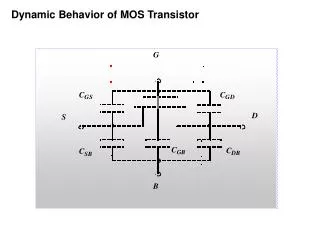
Dynamic Behavior of MOS Transistor MOS Transistor Theory
MOS Transistor Capacitances MOS Transistor Theory
Polysilicon gate Source Drain W x x + + n n d d Gate-bulk L d overlap Top view Gate oxide t ox + + n n L Cross section Overlap Capacitances (F/m2) *Cfringe = (2ox/) ln (1+Tpoly/tox) MOS Transistor Theory
G G G D D D S S S B B B Cut-off Resistive Saturation Gate-Channel Capacitances Most important regions in digital design: saturation and cut-off MOS Transistor Theory