MOS Transistor
MOS Transistor. ECE442: Digital Electronics. SYSTEM. +. G. MODULE. S. D. n+. n+. GATE. CIRCUIT. CIRCUIT. V in. V in. V out. V out. DEVICE. Review: Design Abstraction Levels. The MOS Transistor. Polysilicon. Aluminum.

MOS Transistor
E N D
Presentation Transcript
MOS Transistor ECE442: Digital Electronics
SYSTEM + G MODULE S D n+ n+ GATE CIRCUIT CIRCUIT Vin Vin Vout Vout DEVICE Review: Design Abstraction Levels
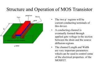
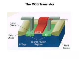
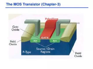
The MOS Transistor Polysilicon Aluminum
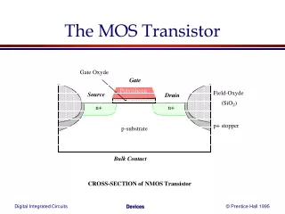
n areas have been doped with donor ions (arsenic) of concentration ND - electrons are the majority carriers L W p areas have been doped with acceptor ions (boron) of concentration NA - holes are the majority carriers The NMOS Transistor Cross Section Gate oxide Polysilicon Gate Source Drain Field-Oxide (SiO2) n+ n+ p substrate p+ stopper Bulk (Body)
Closed (on) (Gate = ‘1’) Open (off) (Gate = ‘0’) Ron Switch Model of NMOS Transistor Gate | VGS | Source (of carriers) Drain (of carriers) | VGS | < | VT | | VGS | > | VT |
Closed (on) (Gate = ‘0’) Open (off) (Gate = ‘1’) Ron Switch Model of PMOS Transistor Gate | VGS | Source (of carriers) Drain (of carriers) | VGS | > | VDD – | VT | | | VGS | < | VDD – |VT| |
VGS + - n+ depletion region n channel Threshold Voltage Concept G D S n+ p substrate B The value of VGS where strong inversion occurs is called the threshold voltage, VT
The Threshold Voltage VT = VT0 + (|-2F + VSB| - |-2F|) where VT0 is the threshold voltage at VSB = 0 and is mostly a function of the manufacturing process • Difference in work-function between gate and substrate material, oxide thickness, Fermi voltage, charge of impurities trapped at the surface, dosage of implanted ions, etc. VSB is the source-bulk voltage F = -Tln(NA/ni) is the Fermi potential (T = kT/q = 26mV at 300K is the thermal voltage; NA is the acceptor ion concentration; ni 1.5x1010 cm-3 at 300K is the intrinsic carrier concentration in pure silicon) = (2qsiNA)/Coxis the body-effect coefficient (impact of changes in VSB) (si=1.053x10⁻¹⁰F/m is the permittivity of silicon; Cox = ox/tox is the gate oxide capacitance with ox=3.5x10⁻¹¹F/m)
The Body Effect • VSB is the substrate bias voltage (normally positive for n-channel devices with the body tied to ground) • A negative bias causes VT to increase from 0.45V to 0.85V VT (V) VBS (V)
- + V(x) ID n+ x Transistor in Linear Mode Assuming VGS > VT VGS VDS G S D n+ B The current is a linear function of both VGS and VDS
Voltage-Current Relation: Linear Mode For long-channel devices (L > 0.25 micron) • When VDS VGS – VT ID = k’n W/L [(VGS – VT)VDS – VDS2/2] where k’n = nCox = nox/tox = is the process transconductanceparameter (n is the carrier mobility (m2/Vsec)) kn = k’n W/L is the gain factor of the device For small VDS, there is a linear dependence between VDS and ID, hence the name resistive or linear region
ID n+ n+ Pinch-off - + VGS - VT Transistor in Saturation Mode Assuming VGS > VT VDS > VGS - VT VGS VDS G S D B The current remains constant (transistor saturates)
Voltage-Current Relation: Saturation Mode For long channel devices • When VDS VGS – VT ID’ = (k’n/2) W/L [(VGS – VT) 2] since the voltage difference over the induced channel (from the pinch-off point to the source) remains fixed at VGS – VT • However, the effective length of the conductive channel is modulated by the applied VDS, so ID = ID’ (1 + VDS) where is the channel-length modulation (varies with the inverse of the channel length)
Current Determinates • For a fixed VDS and VGS (> VT), IDS is a function of • the distance between the source and drain – L • the channel width – W • the threshold voltage – VT • the thickness of the SiO2 – tox • the dielectric of the gate insulator (e.g., SiO2) – ox • the carrier mobility • for NMOS: n = 500 cm2/V-sec • for PMOS: p = 180 cm2/V-sec
1.57V VDS = VGS - VT 1.07V 0.57V 2.07V Quadratic dependence Linear Saturation cut-off Long Channel I-V Plot (NMOS) X 10-4 VGS = 2.5V VGS = 2.0V ID (A) VGS = 1.5V VGS = 1.0V VDS (V) NMOS transistor, 0.25um, Ld = 10um, W/L = 1.5, VDD = 2.5V, VT = 0.43V
Short Channel Effects • Behavior of short channel device mainly due to sat =105 5 • Velocity saturation – the velocity of the carriers saturates due to scattering (collisions suffered by the carriers) Constant velocity n (m/s) Constant mobility (slope = ) c= (V/m) • For an NMOS device with L of .25m, only a couple of volts difference between D and S are needed to reach velocity saturation
Voltage-Current Relation: Velocity Saturation For short channel devices • Linear: When VDS VGS – VT ID = (VDS) k’n W/L [(VGS – VT)VDS – VDS2/2] where (V) = 1/(1 + (V/cL)) is a measure of the degree of velocity saturation • Saturation: When VDS = VDSAT VGS – VT IDSat = (VDSAT) k’n W/L [(VGS – VT)VDSAT – VDSAT2/2]
VGS = VDD Velocity Saturation Effects For short channel devices and large enough VGS – VT Long channel devices • VDSAT < VGS – VT so the device enters saturation before VDS reaches VGS – VT and operates more often in saturation Short channel devices VDSAT VGS-VT • IDSAT has a linear dependence w.r.t VGS so a reduced amount of current is delivered for a given control voltage
Linear dependence Linear Saturation Short Channel I-V Plot (NMOS) X 10-4 Early Velocity Saturation VGS = 2.5V VGS = 2.0V ID (A) VGS = 1.5V VGS = 1.0V VDS (V) NMOS transistor, 0.25um, Ld = 0.25um, W/L = 1.5, VDD = 2.5V, VT = 0.43V
MOS ID-VGS Characteristics • Linear (short-channel) versus quadratic (long-channel) dependence of ID on VGS in saturation • Velocity-saturation causes the short-channel device to saturate at substantially smaller values of VDS resulting in a substantial drop in current drive X 10-4 long-channel quadratic ID (A) short-channel linear VGS (V) (for VDS = 2.5V, W/L = 1.5)
Short Channel I-V Plot (PMOS) • All polarities of all voltages and currents are reversed VDS (V) VGS = -1.0V VGS = -1.5V ID (A) VGS = -2.0V VGS = -2.5V X 10-4 PMOS transistor, 0.25um, Ld = 0.25um, W/L = 1.5, VDD = 2.5V, VT = -0.4V
The MOS Current-Source Model ID = 0 for VGS – VT 0 ID = k’ W/L [(VGS – VT)Vmin–Vmin2/2](1+VDS) for VGS – VT 0 with Vmin = min(VGS – VT, VDS, VDSAT) and VGT = VGS - VT G ID S D B • Determined by the voltages at the four terminals and a set of five device parameters