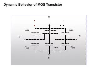
Dynamic Behavior of MOS Transistor
370 likes | 770 Vues
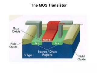
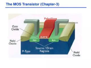
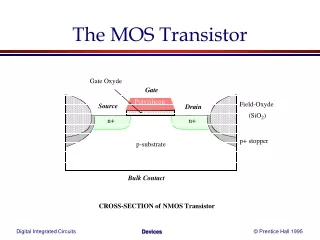
Dynamic Behavior of MOS Transistor. Polysilicon gate. Source. Drain. W. x. x. +. +. n. n. d. d. Gate-bulk. L. d. overlap. Top view. Gate oxide. t. ox. +. +. n. n. L. Cross section. The Gate Capacitance. Gate Capacitance. Cut-off. Resistive. Saturation.

Dynamic Behavior of MOS Transistor
E N D
Presentation Transcript
Polysilicongate Source Drain W x x + + n n d d Gate-bulk L d overlap Top view Gate oxide t ox + + n n L Cross section The Gate Capacitance
Gate Capacitance Cut-off Resistive Saturation Most important regions in digital design: saturation and cut-off
Gate Capacitance Capacitance as a function of the degree of saturation Capacitance as a function of VGS (with VDS = 0)
Diffusion Capacitance Channel-stop implant N 1 A Side wall Source W N D Bottom x Side wall j Channel L Substrate N S A
Define active areas Etch and fill trenches Implant well regions Deposit and pattern polysilicon layer Implant source and drain regions and substrate contacts Create contact and via windows Deposit and pattern metal layers CMOS Process at a Glance • One full photolithography sequence per layer (mask) • Built (roughly) from the bottom up 5 metal 2 4 metal 1 2 polysilicon 3 source and drain diffusions 1 tubs (aka wells, active areas)
Photolithographic Process optical mask oxidation stepper exposure photoresist removal (ashing) photoresist coating photoresist development process step spin, rinse, dry acid etch
Patterning - Photolithography UV light • Oxidation • Photoresist (PR) coating • Stepper exposure • Photoresist development and bake • Acid etching Unexposed (negative PR) Exposed (positive PR) • Spin, rinse, and dry • Processing step Ion implantation Plasma etching Metal deposition • Photoresist removal (ashing) mask SiO2 PR
Chemical or plasma etch Hardened resist SiO 2 Si-substrate Si-substrate Silicon base material 4. After development and etching of resist, chemical or plasma etch of SiO2 Photoresist SiO2 Si-substrate Hardened resist 1&2. After oxidation and deposition of negative photoresist SiO2 Si-substrate UV-light 5. After etching Patterned optical mask Exposed resist SiO2 Si-substrate Si-substrate 8. Final result after removal of resist 3. Stepper exposure Example of Patterning of SiO2
Diffusion and Ion Implantation • Area to be doped is exposed (photolithography) • Diffusion or Ion implantation
Deposition and Etching • Pattern masking (photolithography) • Deposit material over entire wafer CVD (Si3N4) chemical deposition (polysilicon) sputtering (Al) • Etch away unwanted material wet etching dry (plasma) etching
Self-Aligned Gates • Create thin oxide in the “active” regions, thick elsewhere • Deposit polysilicon • Etch thin oxide from active region (poly acts as a mask for the diffusion) • Implant dopant
Simplified CMOS Inverter Process cut line p well
A Modern CMOS Process Dual-Well Trench-Isolated CMOS gate oxide field oxide Al (Cu) SiO2 TiSi2 tungsten SiO2 p well n well p-epi n+ p+ p-
Base material: p+ substrate with p-epi layer p-epi + p Si N 3 4 SiO After deposition of gate-oxide and sacrifical nitride (acts as a buffer layer) 2 p-epi + p After plasma etch of insulating trenches using the inverse of the active area mask p + Modern CMOS Process Walk-Through
SiO After trench filling, CMP planarization, and removal of sacrificial nitride 2 n After n-well and VTp adjust implants p After p-well and VTn adjust implants CMOS Process Walk-Through, con’t
poly(silicon) After polysilicon deposition and etch n + + p After n+ source/dram and p+ source/drain implants. These steps also dope the polysilicon. SiO 2 After deposition of SiO2 insulator and contact hole etch CMOS Process Walk-Through, con’t
Al After deposition and patterning of first Al layer. Al SiO 2 After deposition of SiO2 insulator, etching of via’s, deposition and patterning of second layer of Al. CMOS Process Walk-Through, con’t
Layer Map • Metals (seven) and vias/contacts between the interconnect levels • Note that m5 connects only to m4, m4 only to m3, etc., and m1 only to poly, ndif, and pdif • Some technologies support “stacked vias” • Active – active areas on/in substrate (poly gates, transistor channels (nfet, pfet), source and drain diffusions (ndif, pdif), and well contacts (nwc, pwc)) • Wells (nw) and other select areas (pplus, nplus, prb)
CMOS Inverter Layout Out In metal1-poly via metal1 polysilicon metal2 VDD pfet PMOS (.48/.06 = 12/1) pdif NMOS (.24/.06 = 4/1) metal1-diff via ndif nfet GND metal2-metal1 via or Contact
Simplified Layouts • Calibre for design rule checking (DRC) • FET generation (just overlap poly and diffusion and it creates a transistor) • Simplified via/contact generation • Use the CO (contact) drawing layer • M2X_M1, M3X_M2, M4X_M3, M5X_M4 0.44 x 0.44 m1 0.3 x 0.3 ct 0.44 x 0.44 poly
Design Rules • Interface between the circuit designer and process engineer • Guidelines for constructing process masks • Unit dimension: minimum line width • scalable design rules: lambda parameter • absolute dimensions: micron rules • Rules constructed to ensure that design works even when small fab errors (within some tolerance) occur • A complete set includes • set of layers • intra-layer: relations between objects in the same layer • inter-layer: relations between objects on different layers
Why Have Design Rules? • To be able to tolerate some level of fabrication errors such as • Mask misalignment • Dust • Process parameters (e.g., lateral diffusion) • Rough surfaces
Intra-Layer Design Rule Origins • Minimum dimensions (e.g., widths) of objects on each layer to maintain that object after fab • minimum line width is set by the resolution of the patterning process (photolithography) • Minimum spaces between objects (that are not related) on the same layer to ensure they will not short after fab 0.09 micron 0.045 0.09 micron 0.045
Inter-Layer Design Rule Origins • Transistor rules – transistor formed by overlap of active and poly layers Transistors Catastrophic error Unrelated Poly & Diffusion Thinner diffusion, but still working