Download
1 / 9
110 likes | 301 Vues
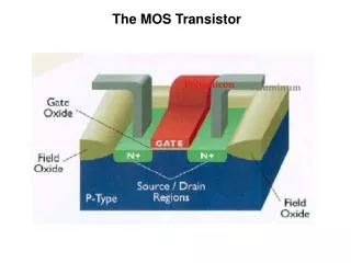
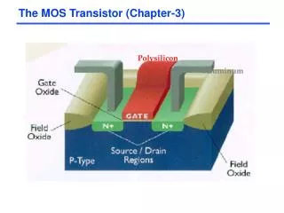
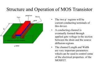
The two p + regions will be current-conducting terminals of this device. A conducting channel is eventually formed through applied gate voltage in the section between the drain and the source diffusion regions.

E N D
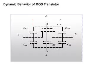
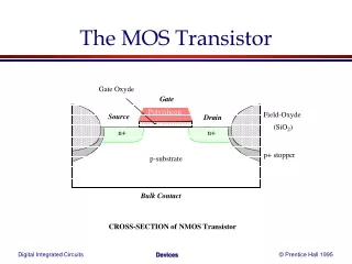
The two p+ regions will be current-conducting terminals of this device. A conducting channel is eventually formed through applied gate voltage in the section between the drain and the source diffusion regions. The channel Length and Width are very important parameters which can be used to control some of the electrical properties of the MOSFET. Structure and Operation of MOS Transistor
The oxide thickness (tox) is yet another important parameter of the MOSFET. An MOS transistor that has no conducting channel region at zero gate bias is called an enhancement-type (enhancement mode) MOSFET. If a conducting channel already exists at zero gate bias the device is called a depletion-type (depletion mode) MOSFET. By definition the terminal voltages of a MOSFET are defined with respect to the source potential. The gate-to-source voltage (VGS), the drain-to-source voltage (VDS), the substrate-to-source voltage (VBS). VDS VGS Gate Oxide Source (n+) Drain (n+) Depletion Region P-type substrate VGS<VT0 The MOS Transistor Structure and Operation
The configuration shown (VDS = VGS =VSB=0) with VGS <VT0 implies that the surface is devoid of mobile carriers and current conduction between the source and the drain is not possible. If the gate-to source voltage is further increased and the surface potential in the channel reaches -ΦFp we get to surface inversion. The channel at this point provides an electrical connection between the two n+ regions. If there is potential difference between the source and the drain terminal voltages current will flow. The bias conditions for the onset of inversion and for the creation of a conduction channel are significant for MOSFET operation. The value of the gate-to-source voltage VGS needed to cause surface inversion is called the threshold voltage (VT0). The MOS Transistor Structure and Operation
Any gate-to-source voltage less than VT0 is not sufficient to establish an inversion layer. The MOSFET conducts no current between its source and drain terminals unless VGS is greater than VT0. Increasing the gate-to-source voltage above and beyond VT0 will not affect the surface potential and the depletion region depth. There are 4 physical properties that affect the threshold voltage namely (i) the work function difference between the gate and the channel, (ii) the gate voltage component to change the surface potential, (iii) the gate voltage component to offset the depletion region charge and (iv) the voltage component to offset the fixed charges in the gate oxide and in the silicon oxide interface. 2FF The Threshold Voltage Oxide (SiO2) P-type Semiconductor (Si) Metal (Al) Ec Ei FF EFp -FF Ev qVT0
The work function difference (Fgate-to-channel) reflects the built in potential of the MOS structure which consists of the p-type substrate, the thin silicon dioxide layer and the gate electrode. FGC = FF(substrate) –FM if the gate material is metal (Aluminum) If polysilicon is the gate material: FGC = FF(substrate) – FF (gate) An externally applied voltage must be changed to achieve surface inversion i.e. to change the surface potential by -2FF. The depletion region charge density at surface inversion (FS = -FF) is QB0=-(2qNASi|-2FF|)-1/2 Assuming that the substrate is biased at a different voltage level than the source (at ground) then the depletion region charge density can be expressed as a function of the source-to-body voltage VSB: QB=-(2qNASi|-2FF|+ VSB)-1/2 The third component offsets the depletion region charge and is equal to –QB/Cox (Cox=ox/tox). The Threshold Voltage
The gate voltage that is necessary to offset to the fixed positive charge density Qox (at the interface between the gate oxide and the silicon substrate) is –Qox/Cox. Combining all the voltage components we can determine the threshold voltage. For zero substrate bias VT0 is given by: VT0=FGC-2FF-QB0/Cox-Qox/Cox Determine the expression for nonzero substrate bias. The most general form of the threshold voltage is: VT=FGC-2FF-QB0/Cox-Qox/Cox-QB/Cox-QB0/Cox VT=VT0-(QB-QB0)/Cox (QB-QB0)/Cox=((2qNASi)-1/2) /Cox*((|-2FF+VSB|)-1/2-(|2FF|)-1/2) This becomes the most general expression of the threshold voltage with the parameter gamma being: The Threshold Voltage
Gamma is called the substrate-bias or the body effect coefficient. The general expression for the threshold voltage can be used for both the n-channel and p-channel devices. The differences are as follows: Substrate Fermi potential FF is negative in nMOS but positive for pMOS. The depletion region charge densities QB0 and QB are negative for nMOS but positive for pMOS Further differences: The substrate bias coefficient g is positive for nMOS and negative for pMOS. The substrate bias voltage VSB is positive in nMOS but negative for pMOS. Typically the threshold voltage of an enhancement mode n-type MOSFET is a positive quantity while that of a p-type MOSFET is negative. The general equation for VT does not provide accurate computations The Threshold Voltage
At VGS > VT0 and VDS = 0 there exists thermal equilibrium in the inverted channel region and the drain current ID = 0. If VDS > 0 (small) is applied the drain current proportional to VDS will flow from source to drain through the conducting channel. This operation is the linear mode. In the linear mode the transistor acts as a voltage-controlled resistor. The channel depth at the drain end of the device starts decreasing. MOSFET Operation: Qualitative View VG > VT VDS (small) VGS=0 IDS Gate Oxide Channel Source (n+) Drain (n+) Depletion Region P-type substrate VG > VT VDS =VDSAT VGS=0 Gate Oxide Channel Pinch-Off Point Source (n+) Drain (n+) Depletion Region P-type substrate VG > VT VDS > VDSAT VGS=0 Gate Oxide Channel Pinch-Off Point Source (n+) Drain (n+) Depletion Region P-type substrate
Eventually VDS=VDSAT the inversion charge at the drain is reduced to zero (pinched off). Beyond pinch-off i.e. VDS > VDSAT a depleted surface region forms adjacent to the drain and this depletion region grows toward the source with increasing VDS. The MOSFET is operating in Saturation Mode (saturation region). The inversion layer near the drain vanishes while the channel end voltage remains constant at VDSAT. The analytical derivation of the MOSFET current-voltage relationships for various bias conditions requires that several approximations be made to simplify the problem. Some assumptions: The threshold voltage along the channel is constant. The electric field is assumed to be dominant along the channel (x-dimension). The entire channel region between the source and the drain is inverted. MOSFET Operation: A Qualitative View