Chapter 18. Non-ideal MOS
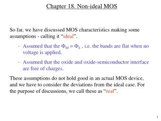
Chapter 18. Non-ideal MOS. So far, we have discussed MOS characteristics making some assumptions - calling it “ ideal ”. Assumed that the M = S , i.e. the bands are flat when no voltage is applied. Assumed that the oxide and oxide-semiconductor interface are free of charges.

Chapter 18. Non-ideal MOS
E N D
Presentation Transcript
Chapter 18. Non-ideal MOS • So far, we have discussed MOS characteristics making some assumptions - calling it “ideal”. • Assumed that the M = S , i.e. the bands are flat when no voltage is applied. • Assumed that the oxide and oxide-semiconductor interface are free of charges. • These assumptions do not hold good in an actual MOS device, and we have to consider the deviations from the ideal case. For the purpose of discussions, we call these as “real”.
Metal-semiconductor work function difference - ideal When M = S , the Fermi level is aligned before we make the device. So, when the MOS structure is made, the band remains flat when the applied gate voltage is zero. Assumption: MS = M – S = 0 S M Flat band condition EFS EFM M O S
M S EFM EFS M = Al M O S Metal-semiconductor work function difference - real M depends on the metal. Example: M (Al) 4 eV, M (Au) 5.1 eV S depends on the semiconductor doping. S = + (EC – EF)FB So, MS = M – S 0 in a “real” device. So, actual band alignment before making the MOS-C structure looks as shown for Al-Si (p)
Band diagram for MS = M – S 0 M S EFM EFM EFS M = Al EFS M O S S We have to apply a gate voltage = MS/q to get flat-band condition.
Polysilicon gate MOS Modern day devices generally use heavily doped polysilicon as the gate material. For p+-polysilicon gate, EFM can be assumed to be at EV. For n+-polysilicon gate, EFM can be assumed to be at EC. Question: If the substrate is intrinsic silicon, and the gate material is p+-polysilicon, calculate MS.(MS = Eg /2 = 0.55 eV) What is the voltage that has to be applied to the gate to get flat-band condition?VG = 0.55 eV/q = 0.55 V Question: If the substrate is n+-silicon, and the gate material is p+-polysilicon, calculate MS.(MS = + 1.1 eV) Show MS by drawing the band diagram.
Interface and oxide charges For the “ideal” device, we have assumed that the oxide and the interface is devoid of any excess charges. This is not true in practice. Assume that all these charges are situated close to the interface on the oxide side (even though they aren’t) and their concentration is Qi (Coulombs/cm2). Qi = net interface charges in C/cm2 Qmetal Na+ Qof Na+ + + -- -- + - Qof Qit + + + + + + + + + + + + + + + + ++ Si
Effect of interface charges, Qi (C/cm2) The interface charge Qi in the oxide (assumed positive) will induce some negative charges (Qi /cm2) in the semiconductor. The effect is as though we have applied a positive gate voltage to the gate, and the negative charges in the semiconductor causes band bending. To get “flat-band” condition, we have to apply a negative voltage to the gate. Voltage to be applied to the gate to get flat-band condition Qi is usually positive (but can be both positive or negative in general).
voltage to be applied to the gate to get flat band condition. = Effects of work function difference and interface charges If we consider the effects of work function difference and the interface charges, the silicon band diagram may not be “flat” even when no voltage is applied to the gate. Hence, a correction has to be applied to the threshold voltage calculations carried out earlier assuming “ideal” MOS conditions. where VT is the threshold voltage assuming ideal conditions (using equation 17.1 in text).
Effects of MS and Qi on CG-VG characteristics of MOS-capacitor CG CG VFB VFB ideal ideal actual actual VG VG p-type n-type A horizontal shift in C-V curve is observed. Routinely used to characterize MOS-C during IC fabrication.
Enhancement and depletion mode MOSFETs Device is “off” when VG = 0 enhancement-mode MOSFET Device is “on” when VG = 0 depletion-mode MOSFET
Threshold adjustment using ion implantation D S B-ion G Boron (+) ions () ions Phosphorous N+ N+ p-type Si = positive shift for acceptor implantation = negative shift for donor implantation Bdose= # of boron ions/cm2 ; Pdose= # of phosphorus ions/cm2
Example 1 Consider an NMOS with oxide thickness of 0.1 m. The threshold voltage measured to be 0.5 V. Calculate the boron or phosphorous ions to be implanted to make VT equal to 2 V. VT = +1.5 V a positive shift. So use boron ions. Calculate density of B ions. (3.2 1011 ions/cm2) During IC fabrication, ion-implantation is routinely used to tailor the the threshold voltage MOSFET device.