Download
1 / 25
330 likes | 861 Vues
Learn about MOS capacitors, from ideal structure to deviation in behavior, with C-V characteristics and charge analysis. Key concepts include gate bias effects, energy band diagrams, and bias regimes. Reference material provided.

E N D
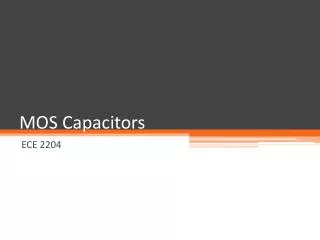
MOS Capacitors • 1. Ideal MOS Capacitor • 2. MOS Capacitor under DC bias (p-type silicon) • 3. MOS Capacitor under DC bias (n-type silicon) • 4. Analysis of the Ideal MOS Structure • 5. Deviation from ideal MOS Capacitor Behaviour • 6. Capacitance – Voltage Characteristics
Expected Outcomes At the end of the lectures on MOS capacitors, you should be able to : • Explain the effects of gate bias on the charge in the MOS capacitor, hence the concepts of accumulation, depletion and inversion; • Draw the energy band diagram of the MOS capacitor at equilibrium and under different bias regimes; • Perform simple analysis such as the calculation of the depletion layer width, flat band voltage, threshold voltage; • Sketch the C-V characteristics and relate the different parts of the curve to the different bias regimes of the MOS Capacitor.
Reading • D A Neamen, Semiconductor Physics and Devices, Third Edition, McGraw-Hill (2003), pp. 449 – 459, 462 – 468, 474 – 480.
1. Ideal MOS Capacitor Basic assumptions for the ideal MOS capacitor : The oxide is a perfect insulator. There are no charges in the oxide or at the oxide-semiconductor interface. [1] [1] This is the basis of the assumption that under any biasing condition the amount of charge on the metal adjacent to the oxide is equal to the amount of the induced charge in the semiconductor but with opposite signs. The case where there are charges in the oxide or at the oxide-semiconductor interface will be considered later.
oxide metal semiconductor When VG = 0, the energy difference between the metal work function m and the semiconductor work function s is zero, i.e., ms = 0.[2] All the energy bands are flat. [2] This assumption is generally not true in real MOS devices. It has only been made at this point to make the descriptionof the static behavior of MOS capacitor simpler, in order to aid out initial understanding of the MOS system.This condition will be relaxed later.
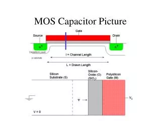
2. MOS Capacitor Under DC Bias (p-type silicon substrate) 2.1 Accumulation (VG< 0) • The schematic diagram shows the cross-section of a MOS capacitor, where the semiconductor is p-type. The majority carriers are holes, and the minority carriers are electrons. Animation of MOS capacitor in accumulation
Negative charges supplied to the gate by the external bias should be balanced by positive charges on the silicon side. Therefore,holes at the silicon surface are induced and the surface of the silicon becomes more p-type. • Since the hole in p-type silicon is the majority carrier and the hole concentration at the interface is higher than that in the silicon substrate, this is a situation of majority carrier “accumulation” condition.
M O S Charge distribution Energy band diagram • When VG is negative, the energy bands in the bulk (interior) of the silicon move downwards, relative to EF in the metal. This results in the bands bending upwards at the Si/SiO2 interface. • But, for an ideal MOS capacitor, no steady state current flows as the oxide is a perfect insulator Fermi level in the silicon remains constant (flat). • Hole concentration : • As (Ei – EF) is larger at the surface than in the bulk, there are more holes (majority carriers) at the surface than in the bulk accumulation.
2.2 Depletion (VG > 0) Animation of MOS capacitor in depletion • Positive charges supplied to the gate repel the free holes in silicon away from the Si/SiO2 interface, which leave behind un-compensated ionized acceptors in the depletion region in the silicon. • The MOS capacitor is said to be in the “Depletion” condition.
M O S Energy band diagram Charge distribution • When VG > 0, the energy bands in the bulk (interior) of the silicon move upwards, relative to EF in the metal. This results in the bands bending downwards at the Si/SiO2 interface. • Hole concentration : • (Ei – EF) is smaller at the surface than in the bulk, thus indicating that holes are depleted at the surface. • The space charge in the depletion layer, per unit area, QD = -eNAW where NA : doping concentration, W : depletion layer width. • Since the positive charge at the gate side should be balanced by the space charge QD in the depletion region, increase of VG (more positive charges at the gate) will increase W (more negative charges in the depletion region)
2.3 Inversion : When a large positive bias is applied (VG >> 0) Animation of MOS capacitor in inversion • Electrons and holes are thermally generated in the depletion layer. The E-field in the depletion layer causes the holes to go into interior (bulk), and the electrons to collect in a thin layer near the silicon-oxide interface. • The MOS capacitor is said to be in the “Inversion” condition, because the surface layer contain more electrons than holes even though the semiconductor is p-type.
M O S Charge distribution Energy band diagram • When VG >> 0, the energy bands at the surface of the silicon bend downwards even more, so that the intrinsic Fermi level Ei at the surface crosses over the Fermi level EF. • Near the surface, EF – Ei > 0. • As The number of minority carriers (electrons) is greater than the number of majority carriers (holes) near the surface. The surface is thus inverted. • The positive charges on the gate are balanced by the silicon charge, Qsi = Qn + QD, where Qn is the inversion charge (made up of electrons), and the depletion charge, QD =-eNAWm (made up of ionized acceptors).
There are two types of inversion : 1. Weak inversion: • The electron concentration at the Si/SiO2 interface is not high.Further increase in gate charge is balanced by increase in both Qn& QD. depletion layer width still increases with increasing VG. 2. Strong inversion: • The electron concentration (ns) at the interface is greater than hole concentration (pb) in the bulk. • Since (EF-Ei) at the surface is greater than (Ei-EF) in the bulk. • If the gate voltage VG is increased further, the energy bands near the surface will try to bend downwards a bit more. This will cause (EF-Ei) to increase, which will in turn cause the electron concentration ns in the inversion layer, and hence Qn (made up of electrons) to increase rapidly. Thus, the incremental positive charge on the gate is balanced entirely by the incremental inversion charge. There is negligible increase in the depletion charge, and hence the depletion layer width W does not increase further.
3. MOS Capacitor Under DC Bias (n-type silicon) Depletion, inversion, and accumulation conditions can be formed in a MOS capacitor with an n-type silicon substrate, too, but with opposite voltage polarities. The operations are analogous to the MOS capacitor with a p-type silicon substrate that was discussion in Section 2.
4. Analysis of the Ideal MOS Structure Energy band diagram of p-type Si in an MOS structure Note : The symbol φS here refers to the potential at the surface of the semiconductor with respect to the bulk. It does not represent the semiconductor work function. Electric potential of p-type Si in an MOS structure
Example 1 Consider an ideal MOS capacitor in which there is no difference in the work functions of the metal and the semiconductor, and no charges in the oxide or at the oxide-semiconductor interface. The semiconductor is p-type and the doping NA = 1016 cm-3. The oxide thickness, tox = 50 nm = 50 x 10-7 cm. Calculate (i) the maximum width of the depletion layer Wm, and (ii) the threshold voltage VTof the ideal MOS capacitor. Take T = 300K, Vt = 0.0259 V, ni = 1.5 x 1010 cm-3.