Drift and Diffusion Current
Drift and Diffusion Current. OUTLINE. Carrier drift and diffusion PN Junction Diodes Electrostatics Reading: Chapter 2.1-2.2. Lecture 1, Slide 2. Dopant Compensation. N-type material ( N D > N A ). P-type material ( N A > N D ).

Drift and Diffusion Current
E N D
Presentation Transcript
OUTLINE • Carrier drift and diffusion • PN Junction Diodes • Electrostatics Reading: Chapter 2.1-2.2 Lecture 1, Slide 2
Dopant Compensation N-type material (ND > NA) P-type material (NA > ND) An N-type semiconductor can be converted into P-type material by counter-doping it with acceptors such that NA > ND. A compensated semiconductor material has both acceptors and donors.
Types of Charge in a Semiconductor • Negative charges: • Conduction electrons (density = n) • Ionized acceptor atoms (density = NA) • Positive charges: • Holes (density = p) • Ionized donor atoms (density = ND) • The net charge density (C/cm3) in a semiconductor is
Carrier Drift Hole velocity Electron velocity Notation: mp hole mobility (cm2/V·s) mn electron mobility (cm2/V·s) • The process in which charged particles move because of an electric field is called drift. • Charged particles within a semiconductor move with an average velocity proportional to the electric field. • The proportionality constant is the carrier mobility.
Velocity Saturation In reality, carrier velocities saturate at an upper limit, called the saturation velocity (vsat).
Drift Current vhtA = volume from which all holes cross plane in time t pvht A = # of holes crossing plane in time t q pvht A = charge crossing plane in time t qpvh A = charge crossing plane per unit time = hole current Hole current per unit area (i.e. current density) Jp,drift = qpvh Drift current is proportional to the carrier velocity and carrier concentration:
Conductivity and Resistivity • In a semiconductor, both electrons and holes conduct current: • The conductivity of a semiconductor is • Unit: mho/cm • The resistivity of a semiconductor is • Unit: ohm-cm
Resistivity Example Estimate the resistivity of a Si sample doped with phosphorus to a concentration of 1015 cm-3 and boron to a concentration of 1017 cm-3. The electron mobility and hole mobility are 800 cm2/Vs and 300 cm2/Vs, respectively.
Electrical Resistance V I _ + W t homogeneously doped sample L Resistance (Unit: ohms) where r is the resistivity
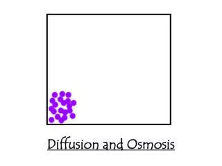
Carrier Diffusion Notation: Dp hole diffusion constant (cm2/s) Dn electron diffusion constant (cm2/s) • Due to thermally induced random motion, mobile particles tend to move from a region of high concentration to a region of low concentration. • Analogy: ink droplet in water • Current flow due to mobile charge diffusion is proportional to the carrier concentration gradient. • The proportionality constant is the diffusion constant.
Diffusion Examples • Linear concentration profile • constant diffusion current Non-linear concentration profile varying diffusion current
Diffusion Current Diffusion current within a semiconductor consists of hole and electron components: The total current flowing in a semiconductor is the sum of drift current and diffusion current:
The Einstein Relation • The characteristic constants for drift and diffusion are related: • Note that at room temperature (300K) • This is often referred to as the “thermal voltage”.
The PN Junction Diode VD – + ID When a P-type semiconductor region and an N-type semiconductor region are in contact, a PN junction diode is formed.
Diode Operating Regions VD = 0 VD < 0 VD > 0 In order to understand the operation of a diode, it is necessary to study its behavior in three operation regions: equilibrium, reverse bias, and forward bias.
Carrier Diffusion across the Junction Notation: nn electron concentration on N-type side (cm-3) pn hole concentration on N-type side (cm-3) pp hole concentration on P-type side (cm-3) np electron concentration on P-type side (cm-3) Because of the difference in hole and electron concentrations on each side of the junction, carriers diffuse across the junction:
Depletion Region quasi-neutral region quasi-neutral region width=Wdep • As conduction electrons and holes diffuse across the junction, they leave behind ionized dopants. Thus, a region that is depleted of mobile carriers is formed. • The charge density in the depletion region is not zero. • The carriers which diffuse across the junction recombine with majority carriers, i.e. they are annihilated.
Carrier Drift across the Junction Because charge density ≠ 0 in the depletion region, an electric field exists, hence there is drift current.
PN Junction in Equilibrium In equilibrium, the drift and diffusion components of current are balanced; therefore the net current flowing across the junction is zero.
Built-in Potential, V0 (Unit: Volts) Because of the electric field in the depletion region, there exists a potential drop across the junction:
Built-In Potential Example N P NA = 1015 cm-3 ND = 1018 cm-3 • Estimate the built-in potential for PN junction below. • Note that

