Download
1 / 12
160 likes | 403 Vues
Chapter 11 Lecture 2--Solids. Metallic Solid Structure Closest Packing = arrangement of atoms to occupy the least space Atoms are spheres that are bonded to each other in all directions There are multiple arrangements to achieve closest packing Hexagonal Closest Packed (hcp)

E N D
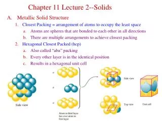
Chapter 11 Lecture 2--Solids • Metallic Solid Structure • Closest Packing = arrangement of atoms to occupy the least space • Atoms are spheres that are bonded to each other in all directions • There are multiple arrangements to achieve closest packing • Hexagonal Closest Packed (hcp) • Also called “aba” packing • Every other layer is in the identical position • Results in a hexagonal unit cell
Cubic Closest Packed Hexagonal Closest Packed
Cubic Closest Packed (ccp) • Also called “abc” packing • Every fourth layer is in the identical position • Results in a face-centered cubical unit cell • Counting atoms • Both hcp and ccp result in each atom having 12 “nearest neighbors” • Six atoms surrounding each atom in the same layer • Three atoms in the layer above and three in the layer below
Counting atoms within the unit cell is important for some applications • For face-centered cubic unit cell (ccp), there are 4 atoms in unit cell • Eight corners, each containing 1/8 of an atom = 1 atom • Six faces, each containing 1/2 of an atom = 3 atoms • Example: Density of ccp Ag with r = 144 pm 4r L
Diamond Metal • Network Atomic Solids: Carbon and Silicon • Properties: directional, covalent bonds, “giant molecules”, brittle, insulators • Carbon Allotropes = different forms of an element in the same state (solid) • Diamond • All carbon atoms sp3 hybridized and tetrahedral • Hardest natural substance known • Insulator: MO diagram has large gap between filled/unfilled MO’s
Graphite • Slippery, black, conductor • All carbons sp2 hybridized and planar • Three directional, covalent s-bonds • Extra p-orbitals form “clouds” above/below carbon planes; this allows electrons to “flow” making graphite a conductor • Lubricant: strong bonding within layers, weak bonding between them
Silicon is a very important component of rocks and minerals • Silica = SiO2 = quartz, sand • CO2 is a gas: sigma and pi bonds between carbon and oxygens • SiO2 is a network solid: Si 3p orbitals too large to overlap with O 2p No pi bonds, so Si forms two more sigma bonds with other O’s Quartz = tetrahedral Si bonded to 4 O’s, empirical formula = SiO2 • Silicates = tetrahedral SiO4 units with O:Si ratios greater than 2:1 Other cations needed to balance the resulting negative charge (Al3+)
Glass = rapidly cooled molten silica (>1600 oC) • Amorphous solid: silica crystal structure doesn’t re-form on cooling • Result is an amorphous solid (glass) rather than crystalline (quartz) • Common Glass: Na2CO3 added to silica • Lab Glass (Pyrex): B2O3 added to silica = doesn’t expand/contract • Lenses: K2O added to silica = harder, maintains precise shape Melt, Rapidly Cool Quartz Glass Quartz Crystal
Ceramics = nonmetallic, silicate clays that are fire hardened • Brittle, strong, chemical and heat resistant • Glass = homogeneous frozen solution (1 phase) • Ceramic = heterogeneous frozen solution (2 phases) • Glassy “cementing” phase • Suspended silicate crystals • Fire hardening removes water, which had allowed clays to “flow” • New “high tech” materials are often ceramics • Semiconductors • Si solid has a structure like diamond, but a smaller MO energy gap • Some electrons can cross the gap at 25 oC = semiconductor • Increasing the temperature increases how conducting it is • Doped Si includes some other element impurities = more conducting • N-type semiconductor = dopant has 1 more electron than Si (As) • P-type semiconductor = dopant has 1 less electron than Si (B) P-type Extra “holes” N-type Extra e-
7. Semiconductors and Electronics • Both n-type and p-type semiconductors are better conductors than Si • Extra electrons make it easier for electrons to cross gap • Extra “holes” mean some unpaired electrons, which conduct better Holes are regarded as positive charge carrier • P-N Junction • Reverse Bias = no current flows = p-type connected to negative terminal and n-type connected to positive terminal • Forward Bias = current flows = p-type connected to positive terminal and n-type connected to negative terminal Electrons can flow from n-type to p-type (extra e- to extra holes) • AC-DC Rectifier: alternating current changed into direct current because electrons only flow during Forward Bias phase
N-type and P-type semiconductors Reverse Bias And Forward Bias In p-n junctions