Download
1 / 38
380 likes | 384 Vues
This workshop focuses on research and educational objectives in the fields of CMP, plasma, diffusion, lithography, and sensors & controls. The session also includes poster sessions and a steering committee meeting. The workshop is organized by Costas Spanos, Jeffrey Bokor, and Andy Neureuther.

E N D
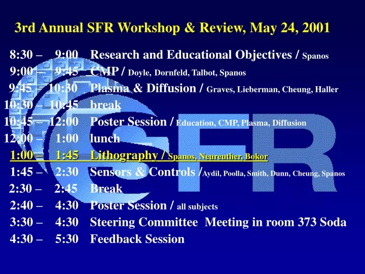
3rd Annual SFR Workshop & Review, May 24, 2001 8:30 – 9:00 Research and Educational Objectives / Spanos 9:00 – 9:45 CMP / Doyle,Dornfeld, Talbot, Spanos 9:45 – 10:30 Plasma & Diffusion / Graves, Lieberman, Cheung, Haller 10:30 – 10:45 break 10:45 – 12:00 Poster Session / Education, CMP, Plasma, Diffusion 12:00 – 1:00 lunch 1:00 – 1:45 Lithography / Spanos, Neureuther, Bokor 1:45 – 2:30 Sensors & Controls /Aydil, Poolla, Smith, Dunn, Cheung, Spanos 2:30 – 2:45 Break 2:40 – 4:30 Poster Session / all subjects 3:30 – 4:30 Steering Committee Meeting in room 373 Soda 4:30 – 5:30 Feedback Session
Lithography SFR Workshop May 24, 2001 Costas Spanos, Jeffrey Bokor Andy Neureuther Berkeley, CA
Outline • Sensitivity of Spectroscopic Scatterometry: Sub-100nm Technology • Process Monitoring and Optimization Using Simulation and Full-profile Metrology • Effects of Line-Edge Roughness on MOSFET Electrical Behavior • DUV ASML 5500/90 Stepper for Novel Lithography • Automated Characterization of Optical Image Quality • Methodology for rapid and accurate simulation of alternating PSM • Resist Resolution Enhancement and Line-end Shortening Simulation
Sensitivity of Spectroscopic Scatterometry: Sub-100nm Technology EM Response Variations Tan Y Simulations for variation in parameter X [X(-),X(Nominal), X(+)] Lambda Profile Parameters Cos D Are Variations Detectable? Lambda NoYes Commercial Equipment Analysis Determine Noise Contributions Tan Y, Cos D Noise Spectrum Which part of the spectrum contains the most information?
Signal averaged over 30 measurements Noise represents 1s standard deviation for each wavelength Empirical formula for signal-to-noise ratio: Noise = 0.412(Intensity)0.632 (R2 Value = 0.937) Signal-to-Noise Ratio for SOPRA Ellipsometer • Intensity fluctuation is the main contributor of measurement noise in ellipsometers. • Monte-Carlo simulations incorporating intensity fluctuations are used to determine the final distributions of Tan Y and Cos D. • The ‘Minimum Detectable Variation’ lines represent the sum of the 3s errors of each of the 2 profiles measured to obtain the variation. • The graphs demonstrate a trend toward significant information contained in a narrow band in the lower wavelength spectrum.
Detectable (Above yellow line) Undetectable (Below yellow line) 70nm Technology Simulations 70nm Dense Lines (ASIC) 45nm Isolated Lines (MPU)
50nm Technology Simulations 50nm Dense Lines (ASIC) 30nm Isolated Lines (MPU) Detectable (Above yellow line) Undetectable (Below yellow line)
Scatterometry Milestones • Characterize the capabilities of scatterometry in fulfilling the needs of the 100nm technology node, by 9/31/2001- Done! • Feasibility of 100nm profile extraction using small footprint, in-line spectroscopic ellipsometry, by 9/31/2002 • Lithography controller that merges full profile in-line information with available metrology, by 9/31/2003
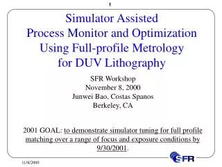
DUV Photolithography In-Line Scatterometry PR Deposition, Focus, Exposure, Bake Time, Development Time, etc Profile Diagnostics Wafers Process Flow Process Flow Process Monitoring and Optimization Using Simulation and Full-profile Metrology Feedback Control Loop
Noise Noise The Lithography Control Framework Using Scatterometry Control parameter Patterned wafer Lithography module Ellipsometer +/- Adjusted offset Measured spectrum Feedback controller Measured profile Scatterometry library Control param. extractor Extracted control parameters
Noise The Simulation Framework For Process Control Using Scatterometry Control parameter Patterned wafer Prolith process simulator Grating response simulator +/- +/- Adjusted offset Measured spectrum Feedback controller Measured profile Scatterometry library Control param. extractor Extracted control parameters
Structure, Profiles and Spectrum: Process Simulation and Scatter Predictions match well 480 nm 160 nm Resist 505 nm ARC 61 nm
Parameter Disturbance Emulating Process Drift First order integrated moving average disturbance model ( = 0.3)
Extracted vs. Input Focus and Exposure Settings: Full Profile Extraction detects process inputs Standard deviation of detection error: 0.025 m (focus), 0.23 mJ/cm2 (exposure)
Control Conclusions and Future Work • Focus and exposure drifts can be monitored with scatterometry. • CD and sidewall angle variations are reduced by feedback control of focus and exposure according to simulation. • Next: • Study the effect of noise and modeling deficiencies on control results. • Study the case of multi-wafer delay between metrology and control. • Original Milestones: • Simulator tuning for full profile matching over a range of focus and exposure conditions, by 9/30/2002 (on target) • Simulator tuning for full statistical profile matching over a range of conditions, by 9/30/2002. • Implement lithography controller that merges full profile in-line information with available metrology, by 9/30/2003.
Effects of Line-Edge Roughness on MOSFET Electrical Behavior SFR Workshop November 8, 2000 Shiying Xiong, J. Bokor EECS of UC-Berkeley Qi Xiang, Philip Fisher AMD Strategic Technology Group
Motivation • Several possible LER effects have been predicted from device simulations • Increase of leakage and driving current • Variation of Vt • Effect on lateral diffusion and doping profile (high frequency effect) • An efficient way to determine these effects in advanced MOSFETs has not been established • Experimental data from devices with different LER needs to be obtained to make a meaningful comparison with simulation results
Motivation • Several possible LER effects have been predicted from device simulations • Increase of leakage and drive current • Variation of Vt • Effect on lateral diffusion and doping profile (high frequency effect) • An efficient way to determine these effects in advanced MOSFETs has not been established • Experimental data from devices with different LER needs to be obtained to make a meaningful comparison with simulation results
LER Experiments with AMD • Characterize LER on AMD wafers and develop ways to vary LER • We have developed methods to measure and characterize LER • AMD results so far has not given reliable increase of LER • Need to work harder to increase LER for the study purpose • Simulate LER effect on AMD device using our method – DONE! • AMD fabricates devices with different LER values • Comparison of experimental data with simulation results
Summary • Poly line width RMS on AMD wafers: 1.5nm~4.5nm • Roughness correlation length, Lc is generally greater than 25nm • HF LER effects are insignificant • Our simulations suggest that the AMD prospective 50nm technology is insensitive the typical LER produced in their process. • We need to produce LER with 4-6nm RMS to test our model Milestones • AMD will fab devices with controlled roughness in this June • Shiying will perform device characterization and comparison with simulation (Fall ’01)
DUV ASML 5500/90 Stepper for Novel Lithography SFR Workshop May 24, 2001 SFR:Andrew R. Neureuther, Mosong Cheng, Haolin Zhang SRC/DARPA Garth Robins, Mike Williamson, Lei Yuan Microlab: Sia Parsa, Kim Chan, Evan Stateler, Bob Hamilton MEMS: Sunil Behave, Richard Yeh Berkeley, CA 2001 GOAL: Complete initial simulations and experiments sufficient to design polarization masks and multi-parameter test structures 9/30/2001 (On Target: tool installed).
ASML 5500/90 Tool and Track Light path Mask Port • Donated/installed by ASML with Cymer laser support • (including unanticipated costs of $75K) • Operational May 4, 2001 with 0.25 mm images • Some track issues being resolved
Special Test Mask and First Wafer Running UCB Mann 3600 and Photo Sciences versions LER Determination Test Mask Electrical Test Double Exposure Gratings Aberration Targets Basic Resolution
Phase-shifted spillover Polarization adjusted half-tone Polarization orthogonal spillover 2002 and 2003 Goals Fly’s eye Hexagonal light pipe Aberration Targets Slit for apodizing Flexible Illumination Conduct and quantitatively interpret polarization masks, and multi-parameter test structures, by 9/30/2002. Define apparatus, specify testing procedures, and interpret data for polarization masks, and multi-parameter test structures, by 9/30/2003.
Automated Characterization of Optical Image Quality Programmed-Probe Based Aberration Targets Dark Field Patterns Grid is 0.1 l/NA Probe Astigmatism ARN on SMART Garth Robins on SRC/DARPA Spherical 1 at 90o Trefoil Coma 1 at 180o 1 at 0o 2001 GOAL: Complete initial simulations and experiments sufficient to design polarization masks and multi-parameter test structures 9/30/2001. (On Target: Thy, Sim done, Exp in progress)
Model for Aberration Target Design and Measurement • Huygen’s Principle and the Fraunhofer (far field) give (x,y) are wafer and (r,q) are lens pupil coordinates • Assuming mask diffracted fields are Zernike’s gives • Mask targets are inverse Fourier transform of Zernike’s • E-field and Intensity at target center of Additive term proportional to the aberration level and quality of the target. Ideal Probe
Ideal Target Examples: Rotationally Symmetric Defocus (Z3) Spherical (Z8) Null on-axis Radius of peak is 0.54 l/NA Radius of peak is 0.84 l/NA
Novel Targets to Distinguish Defocus and Spherical 0.1 wave defocus 0.03 Z8 and Z15
Phase-shifted spillover Polarization adjusted half-tone Polarization orthogonal spillover 2002 and 2003 Goals Aberration Targets Measure with CD SEM Electrical Test Haolin Zhang and Costas Spanos Garth Robins on SMART Conduct and quantitatively interpret polarization masks, and multi-parameter test structures, by 9/30/2002. Define apparatus, specify testing procedures, and interpret data for polarization masks, and multi-parameter test structures, by 9/30/2003.
k+1 k0 k-1 Modeling and Simulation (Mask): Methodology for rapid and accurate simulation of alternating PSM Kostas Adam 100 nm feature with 180 opening 193 nm, NA = 0.6-0.7, s =0.3, 4X By adjusting the complex diffracted orders the thin mask within the NA of the objective is better than 0.5%! Adam SPIE 4346 2001 GOAL: to demonstrate accuracy and generality of simulation method for application to other mask technologies by 9/30/2001. (Done and pursuing further enhancements)
y x Fast Simulation: 90o/270o contact alt. PSM CD=150nm(1X), 1:1.5 4 3 270o 90o Ey (TE) 3mm (4X) 2 1 90o 270o 3mm (4X) • The modified mask transmission function is determined independently for the x- and y- directions => f(x,y) = f(x)f(y) • A few (1-4, TE and TM) 2D rigorous EM simulations (~8min) • A full 3D rigorous EM simulation requires many hours • Accuracy 99% at 100X computational speed-up Adam SPIE 4346
Scatterning from the Phase-Well Corner After vertical wave subtracted l=193nm Ey (TE) 1 n=1 39.7o n=1.563 Front 2 Sources of cross-talk! Adam SPIE 4346
k+1 k0 d k-1 (mm) 2002-2003 Goals “At Mask”Modeling and Simulation PSM Masks and 3D Defects Kostas Adam Extend k-space modeling 3D defects interacting with features and establish defect printability guidelines. Establish guidelines for 3D defect sizing and feature interactions by 9/30/2002. Extend defect modeling to relate inspection to printing 9/30/2003.
Imaging Model < Base PEB Model < Tuned PEB Model Novel technologies and Modeling and Simulation (Wafer): Resist Resolution Enhancement and Line-end Shortening Simulation Mosong Cheng 2001 GOAL: to investigate the impact of electric-field-enhanced post exposure baking on resist profile; validate resist/lens aberration-based line-end shortening model by 9/30/2001.(On Track)
Resist E photoacid Electric-Field-Enhanced Post Exposure Bake • Electric-Field-Assisted Top Surface Imaging: a potential solution of resist to enable short-wavelength lithography. Generate acid at the resist surface, induce reaction in bulk resist by EFE-PEB. • EFE-PEB applied to optical exposure. Invention disclosure filled 4/20/01
2002 and 2003 Goals “At Wafer” Involves “At Wafer” aspects of both task 1.1) Novel Technologies and 1.2) Modeling and Simulation Mosong Cheng Investigate the impacts of the applied electric field polarity, frequency and magnitude on post exposure bake on e-beam and DUV exposure tools by 9/30/2002. Optimize the electric-field-enhanced post exposure baking process by 9/30/2003. Complete the resist/lens aberrations-based line-end shortening model and validate the simulation in 248nm and 193nm lithography by 9/30/2002. Enable 3D EM simulation of substrate topography effects by 9/30/2003.