Download
1 / 33
330 likes | 403 Vues
Explore Scanning Tunneling Microscope (STM) and Atomic Force Microscopy (AFM) block diagrams, dendritic growth, research findings, and operational modes in nanoscience. Discover how these technologies offer insights into surface structures on an atomic scale, chemical contrast, and dynamic processes at nanometer resolution. Read about the use of STM in investigating chemical reactions and phase transitions, with applications in various fields. Uncover the principles behind AFM, its modes of operation, and applications in metrology, fabrication, and biological studies. Enhance your understanding of nanotechnology using these powerful microscopic tools.

E N D
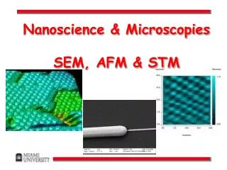
Nanoscience & Microscopies SEM, AFM & STM
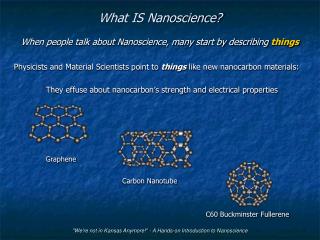
SEM Picts Dendritic Growth Ostrinium Nubilialis
Miami Research Results
STM • Scanning tunneling microscope
Outside the Barrier Wavefunction extends outside of well edge for a finite square well
Two finite wells at a distance • The electron wavefunctions extend into space between finite wells http://www.chembio.uoguelph.ca/educmat/chm729/STMpage/stmdet.htm
Two finite wells at close approachcan look like a barrier to the electrons! • Electrons can tunnel into or through barriers depending on… http://phys.educ.ksu.edu/vqm/html/qtunneling.html
Two finite wells at close approach • Electron wavefunctions can overlap http://www.chembio.uoguelph.ca/educmat/chm729/STMpage/stmdet.htm
This is the STM image of Si(111)-7x7 surface, the white spots represents the position of the atoms.
Scanning -- • Constant Current Mode • Constant Height Mode • http://www.surfaces.lsu.edu/STMoverview.html
Modes of Operation • Constant Current • Constant Height userpage.chemie.fu-berlin.de/.../html/node5.htm
Use of STM- Chemical Constrast The surface of alloys may differ in several respects from the corresponding bulk structure. The surface may also exhibit a chemical order different from the one in the bulk of the material. This influences processes such as gas adsorption and catalysis, since adsorbed molecules often prefer a certain chemical environment of substrate atoms. It all started with an (111) oriented surface of a PtNi alloy (bulk composition 25% Pt, 75% Ni; surface approx. 50% of each). We found that we can distinguish between Pt and Ni atoms on this surface with the STM!Since Pt and Ni are about 50% of the surface atoms each, the brighter species is Ni. The white blobs in the image are impurities of unknown nature. http://www.iap.tuwien.ac.at/www/surface/STM_Gallery/chemical_resolution.html
Excitation of different vibrational modes depending on species (C2H2 vs. C2D2) Science, 280, 1715 (1998). Single molecule chemical reactions Science News, 158, 215 (2000). Use of STM
Researchers usually compare "before" and "after" pictures of typical regions of a material to see how it changes during a phase transition. This is now see on an atomic scale. As the lead atoms in this 20 x 13 nanometer region are warmed from 40 to 136 Kelvin, they switch from the corrugated to the flat arrangement at the transition temperature of 86 Kelvin . Vienna University of Technology
Requires electrical path – for tunneling Gives information of heights of electron clouds above surface – eg. graphite structure Some questions cannot be explored Downside to STM?
Other cool sites… • http://www.almaden.ibm.com/vis/stm (Interesting STM images) • http://www.nobel.se/physics/educational/microscopes/scanning/ (Interesting STM images)
AFM • Cantilever structure on end on end of wafer holds the pyramidal tip • Light from a diode laser bounces of tip and strikes a split photodetector • Motion is detected by differences in intensity on the detector portions http://www.stolaf.edu/depts/physics/afm/diagram.html Let’s also look at: http://www.weizmann.ac.il/Chemical_Research_Support/surflab/peter/afmworks/
Wafer & TIP • Si or SiN – 10 nm at end – ~100 atoms Electron micrograph of two 100 µm long V-shaped cantilevers (by Jean-Paul Revel, Caltech; cantilevers from Park Scientific Instruments, Sunnyvale, CA). • Three common types of AFM tip. • normal tip (3 µm tall); (b) supertip; (c) Ultralever (also 3 µm tall). • Electron micrographs by Jean-Paul Revel, Caltech. http://stm2.nrl.navy.mil/how-afm/how-afm.html
Contact Low and High Gain Low gain – “drag” tip across sample see deflection which is OK for relatively flat surfaces High gain – tries to push down on sample to maintain a particular height which is OK for more bumpy surfaces, but not for soft surfaces - Tapping mode Good for local surface distortions to measure friction and spring forces on surfaces Non-contact Requires a frequency modulation technique which is good for biological samples- repulsive forces from surface AFM Modes
Metrology -- Fabrication • AFM can be used to study the success of e-beam lithography and subsequent processing steps. Nanotechnology, 13 659 (2002).
Microscopic techniques which give us resolutions in angstroms or nanometers Used for fabrication, chemical and biological studies A definite “force” in the nanoworld ! STM & AFM