Download
1 / 20
220 likes | 433 Vues
Introducing concepts of nanoscience and nanotechnology for engineering education. Sandra M. Mendoza. Universidad Tecnológica Nacional – Facultad R egional Reconquista Consejo Federal de Investigaciones Científicas y Técnicas. Outline. Introduction The challenge

E N D
Introducing concepts of nanoscience and nanotechnology for engineering education Sandra M. Mendoza Universidad Tecnológica Nacional – Facultad Regional Reconquista Consejo Federal de Investigaciones Científicas y Técnicas.
Outline • Introduction • The challenge • Objectives of the course • Audience • Course content • Didactical strategies and resources • Conclusions
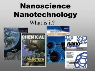
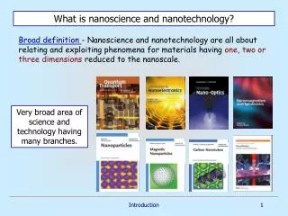
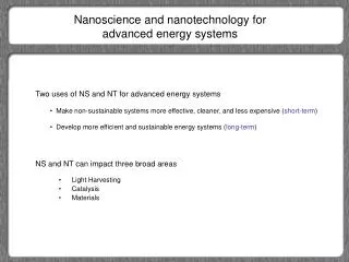
Introduction Nanoscience is the study of matter in the nanometer range. Nanotechnologycomprises the set of techniques developed for the study, manipulation and control of matter in the same range with applications in the real world.
Introduction Nano-related research has strong multidisciplinary roots Position of nanoscience and nanotechnology topics over a base map of science. Each node is one of 175 subject categories in the SCI database, and the size of the node is proportional to the number of papers published in each. http://gtresearchnews.gatech.edu/mapping-nanotechnology/
The challenge Engineering education
Objectives of the course Engineering Scientific basic knowledge Applications Complementing the engineering formal education in the field of advanced materials and nanotechnology, from a practical and applied point of view. • Selecting and applying the scientific knowledge in order to find solution for technological problems. • Understanding the scientific ‘nano-language’ to enhance the communication between researchers, engineers and society, i.e. to be the link between science and solutions in this field of fast development. • Getting constantly updated, with regards to new trends in advanced materials. • Learning about intellectual property, form scientific publications to patents and technology transfer.
Audience Undergraduate students Complete basic university education in mathematics (calculus, arithmetic and analytical geometry), physics, chemistry, thermodynamic and statistics. Careers such as materials, nuclear or chemical engineering. But also mechanical, electrical, biological and civil engineering can be enriched by the course.
Course content • Ultra highvacuum (UHV) technology • Solidstatephysicsforengineering • Surfacescience and thin films • Molecular devices and machines • Samplecharacterization • Microscopytechniques • Spectroscopytechniques • Miscellaneous
Ultra high vacuum (UHV) technology • Vacuum operational ranges. • Vacuum pumps and functioning principles (ionic, sublimation, diffusion, rotary, and more). • Benefits and requirements. • Operational methods. • Applications.
Solid state physics for engineering • Crystalline (surface) structure. • Size-depending properties. Energy bands. • Nanoparticles. • Quantum dots.
Surfacescience and thin films • Monolayers. Multilayers. • Physical vapour deposition (PVD). • Chemical vapour deposition (CVP). • Self-assembly. • Langmuir-blodget technique. • Electron/ion sputtering. Depth profiling. • Some case studies: graphene, alcanothiols, single and multiple walled carbon nanotubes (SWCNT and MWCNT), other fullerenes • Current and prospective applications. Surface science and thin films Thin-Film Batteries for Direct Integration into Electronic Devices Thin film solar panel
Molecular devices and machines • Supramolecular chemistry for engineers. • Functional molecules, nanodevices a ndnanomachines. • Electronic devices, MEMS, NEMS. • Photonic materials. • Introduction to nanoengineered materials. • New trends in material science. microelectromechanicalsystems chip Encapsulation technology and controlled release Graphene and fullerenes
Sample characterization • Microscopy probe techniques: STM), AFM, SEM, TEM. • Spectroscopytechniques: Synchrotronsources, XPS, AES, FT-IR, Raman spectroscopy. Electron energy loss spectroscopy (EELS and HREELS). • Miscellaneous: Surface selective diffraction techniques. Low energy electron diffraction (LEED). Contact angle. Break junction. Theoretical simulation methods. STM Image showing graphite (HOPG) atoms XPS spectrum of goldsubtrate Synchrotron Soleil (France)
Methodology: didactical strategies and resources The course must be in line with the curricular design, norms and rules of the university career where it will be incorporated. • Lectures, by experts in the field. • Experimental sessions where the student will be able to see, apply and get familiar with advanced technology available in material science centers and laboratories, as well as high-tech industries. • Testimonies of professionals who are active in the field
Methodology: didactical strategies and resources • The list of didactical materials includes: • A selection of text books and a specially edited syllabus • Complementary texts. • Access to international publications and patents • Guides for experimental sessions • Authorized simulation software • Laboratory facilities • Online-conference facilities, in order to enrich lectures and laboratory tutorials with the expertise of professionals, who are geographically distant from the course location. • PC, projector, blackboard/whiteboard.
Conclusions • Nanoscience and Nanotechnology are emerging disciplines of science and technology that integrate a broad range of topics. Alternative tool to provide solutions • New engeneering challenges • Disciplines usually not included in formal engineering education (undergradue level) • Curriculum proposal advocated to complement formal education of engineering careers in the field of nanoscience and nanotechnology. Skills for solving technological problems making use of nanotechnology • Impact on future engineers
Acknowledgments • Universidad TecnológicaNacional – Facultad Regional Reconquista • Consejo Federal de InvestigacionesCientíficas y Técnicas (CONICET) • WEEF Comettee
State of the art The first nanoengineering program in the world was started at the University of Toronto within the Engineering Science program as one of the Options of study in the final years. In 2003, the Lund Institute of Technology started a program in Nanoengineering. In 2004, the College of Nanoscale Science and Engineering(CNSE) was established on the campus of the University at Albany. In 2005, the University of Waterloo established a unique program which offers a full degree in Nanotechnology Engineering. Louisiana Tech University started the first program in the U.S. in 2005. In 2006 the University of Duisburg-Essen started a Bachelor and a Master program NanoEngineering. The University of California, San Diego followed shortly thereafter in 2007 with its own department of Nanoengineering. In 2009, the University of Toronto began offering all Options of study in Engineering Science as degrees, bringing the second nanoengineering degree to Canada. DTU Nanotech - the Department of Micro- and Nanotechnology - is a department at the Technical University of Denmark established in 1990.