Download
1 / 14
290 likes | 934 Vues
Surface States of Si(111) Surface. Vildana Hodzic ENEE 697 Project Spring 1999. Surface States of Si(111) Surface. Introduction Si(111) surface structure - Ideal versus real surfaces - Real surfaces: 7x7 reconstruction of Si(111)7x7 surface - Dimer-Adatom-Stacking-Fault Model

E N D
Surface States of Si(111) Surface Vildana Hodzic ENEE 697 Project Spring 1999
Surface States of Si(111) Surface Introduction Si(111) surface structure - Ideal versus real surfaces - Real surfaces: 7x7 reconstruction of Si(111)7x7 surface - Dimer-Adatom-Stacking-Fault Model - Surface density of states and band banding - Fermi level pinning at Si(111)7x7 surfaces - Theoretical work on surface states of Si(111)7x7 Preparation of clean Si(111)7x7 surfaces Theory of observation and experimental data
Introduction • The reliability and stability of all semiconductor devices are closely related to their surface conditions. Therefore, an understanding of the surface physics is of great importance to device operation. Investigating surface electronic properties is also very important since with the downscaling of electronic devices the surface effects become larger as their scale becomes smaller. • The surface of a crystalline solid in vacuum is generally defined as a few (approximately three) outermost atomic layers of the solid that differ significantly from the bulk. It may be atomically clean or it may have foreign atoms deposited on it or incorporated on it. A complete characterization of a solid surface requires knowledge of not only what atoms are present but also where they are. Just as in the bulk, it is not the atomic coordinates as such that are of much direct interest. We are interested in electronic and magnetic properties of the surface and it is the geometrical arrangement of the surface atoms that largely determines the surface charge and spin density. • One can start by thinking of a clean surface in terms of a zero-order approximation, the so-called "ideal surface". That is an abstraction created by passing a plane through an infinite crystal and separating the two parts to infinity without perturbing positions of the atoms and the electron density. "Ideal surfaces" as such do not exist in nature. All surfaces are energetically unfavorable in a sense that they have a positive free energy of formation. A highly unstable or metastable state occurs when covalent bonds are broken by cleavage. The surface atoms undergo relaxation and reconstruction in order to reduce the surface free energy. Both relaxation and reconstruction may occur with clean surfaces in ultrahigh vacuum, but adsorption of species onto the surface may enhance, alter or even reverse the process. • The differences between the real structure of the clean surface and the ideal structure may be imperceptibly small (e.g. a very slight surface relaxation) or much more marked and involving a change in the surface periodicity in one or more of the main symmetry directions (surface reconstruction).
Ideal versus real surfaces The ideal surfaces of the diamond lattice each expose hybrid orbitals that “dangle” into the vacuum. Every such orbital is half-occupied if we imagine that the two bonding electrons/orbital of the bulk are shared between the two half-crystals formed by cleavage. The (111) surface contains one dangling hybrid per surface unit cell. From Fig.1a ) we see that the areal density of dangling hybrids is lowest for the (111) surface. The surface tension of the (111) face is lowest. This is the natural cleavage plane for Si. 1. Harrison,W.A., Electronic Structure and the Properties of Solids, San Francisco: W.H. Freeman, (1980). 2. Ivanov,I., Mazur,A. and Pollmann,J., ”The ideal (111), (110) and (100) surfaces of Si, Ge and GaAs; a comparison of their structure”, Surf.Sci. 92, 365 (1980).
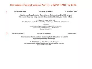
Real surfaces: 7x7 reconstruction of Si(111) surface Clean (111)-oriented Si surfaces prepared by cleavage and subsequent heating to at least 650K in ultra-high vacuum reconstruct into the famous Si(111)7x7 surface structure.Studies of the surface crystallography by LEED back in 1959 revealed that this surface exhibits large surface mesh [3]. The first comprehensive structure analysis of the Si(111)7x7 reconstruction was performed by evaluating intensity distribution of the spots in the TED patterns [4]. This resulted in the Dimer-Adatom-Stacking-Fault model. TED typically uses 100 keV electrons so that the single-scattering approximation can be assumed. Fig.2 Low-energy electron diffraction (LEED) pattern of the Si(111)7x7 reconstruction [3]. Fig.3 Transmission electron diffraction (TED) pattern of the Si(111)7x7 [4]. 3. Schlier,R.E. and Fransworth,H.E.,J.Chem.Phys. 30, 917 (1959). 4. Takayangi,K.,Tanishiro,Y.,Takahashi,S. and Takahashi,M., ”Structure analysis of Si(111)-7x7 reconstructed surface by transmission electron diffraction”, Surf. Sci. 164, 367 (1985).
Dimer - Adatom - Stacking - Fault Model DAS model of the Si(111)7x7 reconstruction is shown schematically in Fig.4 [4]. The non-reconstructed (111) cell corresponding to the 7x7 unit cell contains 49 atoms which are all in the surface plane.In the DAS model the energy associated with the dangling bonds is decreased by reducing their number from 49 to 19. The top layer contains 12 atoms (the so called adatoms) while the layer below consists of 42 atoms. Due to their position, all adatoms are not electronically equivalent.Because of a stacking fault in the unit cell, the two triangular halves are not equivalent and are referred to as faulted and unfaulted halves. Furthermore, one notices that the reconstruction is accompanied by very large angular distortions. The dangling bonds saturated by the adatoms, and the dimer bonds are such examples. These distortions extend in depth to the third layer below the surface. Fig.4. Atom arrangement on Si(111)7x7 surfaces according to the dimer-adatom-stacking-fault (DAS) model [4].
A major breakthrough in surface science occurred after the invention of the Scanning Tunneling Microscope (STM) in 1982 by Binnig et al. [5],[6]. The first atomically resolved STM imaging of Si(111)7x7 surface was achieved a year later [7]. Atomically resolved Atomic Force Microscope (AFM) imaging of Si(111)7x7 surface was the next powerful tool used for studying this surface [9]. Fig. 5 Topographic image of Si(111)7x7 surface as recorded using Scanning Tunneling Microscope (STM) with a bias voltage of + 2 V [8]. Fig. 6 A 3D image of ac-mode Atomic Force Microscope (AFM) data of the Si(111)7x7 surface [9]. 5. Binnig,G., Rohrer,H., Gerber,Ch. And Weibel,E., Physica 107 A&B, 1335 (1982). 6. Binnig,G., Rohrer,H., Gerber,Ch. And Weibel,E., Appl. Phys. Lett. 40, 178 (1982) 7. Binnig,G., Rohrer,H., Gerber,Ch. And Weibel,E.,”7x7 Reconstruction on Si(111) Resolved in Real Space”, Phys. Rev. Lett. 50, 120 (1983). 8. Wiesendanger,R., Tarrach,G.,Scandella,L. and Gunthererodt,H.-J., Ultramicroscopy 32, 291 (1990). 9. Erlandsson,R. and Olsson,L., Appl. Phys. A 66, S879 (1998).
Surface density of states and band bending a) Electronic properties of Si(111)7x7 surface have been analyzed using different techniques: photoemission [10], [11]; electron energy-loss spectroscopies [12],[13]; scanning tunneling microscopy [14],[15]. Angle-resolved photoemission studies have consistently reported the existence of three surface-state bands. The two bands closest to the Fermi level EF (S1 and S2) are interpreted as dangling-bond and the third is associated with back-bonds. The S1 and S2 bands show only a weak dispersion [10]. This has been verified in STM studies [15]. The S1 state, at -0.35eV (relative to EF), is located on adatoms and S2, at -0.8eV, is located to the rest atom positions and at the corner-hole atoms. Photoemission shows significant emission at EF implying that Si(111)7x7 surface is metallic. Low-temperature (55K) photoemission study [11] shows a previously undetected surface-state structure (S’1) at ~0.5eV below EF. It is assigned to dangling-bond states located mainly at the adatoms near the corner holes. b) c) d) Fig. 7 Difference STM images of occupied surface states on a Si(111)7x7 surface:a) topographic image;b) adatom states at -0.35eV;c)dangling bond states at -0.8eV;d)back bond states at -1.7eV [15].
Fig.8 Angle-resolved spectra obtained from the Si(111)7x7 surface at three different sample temperatures.The new surface state S’1 appears in the low- temperature spectra at ~0.5eV below EF [11]. Fig. 9 Photoemission spectra obtained for various emission angles along -M direction of the 1x1 surface Brillouin zone (SBZ) [11]. Fig. 10 Dispersion of the S1 ,S’1 and S2 surface states along the -K and -M symmetry lines of the 1x1 SBZ [11]. 10. Martensson,P.,Ni,W.-X.,Hansson,G.V.,Nicholls,J.M. and Riehl,B., Phys.Rev B 36, 5974 (1987). 11. Uhrberg,R.I.G.,Kaurila,T..Chao,Y.-C.,”Low-temperature photoemission study of the surface electronic structure of Si(111)7x7”,Phys.Rev.B 58, R1731 (1998) 12. Demuth,J.E.,Persson,B.N.J. and Schell-Sorokin,A.J., Phys.Rev.Lett. 51, 2214 (1983). 13. Demuth,J.E.,Persson,B.N.J. and Schell-Sorokin,A.J., Phys.Rev. B 30, 5968 (1984). 14. Wolkow,R. and Avouris,Ph., Phys.Rev.Lett. 60, 1049 (1988). 15. Hamers,R.J.,Tromp,R.M. and Demuth,J.E., Surf. Sci. 181,346 (1987).
Fig. 11 a) Dispersion of surface states on Si(111)7x7 surfaces. S1 to S4 data for occupied states from[10] and U1 data for empty states from [16].Shaded areas indicate surface-projected bulk valance bands; b) Local density of states of restatoms (R), at adatoms near to the corner holes (Ach) and in the center of the unit mesh (Ac) as well as at corner-hole atoms (C) of the Si(111)7x7 DAS structure [17]. 16. Nicholls,J.M. and Reihl,B., Phys. Rev. B 36, 8071 (1987). 17. Brommer,K.D., Galvan,M., Dal Pino,A. and Joannopoulos,J.D., Surf. Sci. 314, 57 (1994).
Theoretical work on surface states of Si(111)7x7 Theoretical work on Si(111)7x7 surface mainly deals with the details of its reconstruction geometry and not nearly as much with detailed calculation of the surface band structure. A detailed analysis of this surface electronic structure is presented in [19]. It is based on the local density approximation (LDA) [18]. The occupancies of different dangling-bonds associated with rest atoms,the corner-hole atom, and the adatoms are analyzed. Their results show that the adatom-dangling bonds control the electron DOS at the Fermi level. Based on the main results obtained in the LDA calculation a two-dimensional Hamiltonian is introduced to describe the correlation properties of the electrons localized in the surface adatom dangling bonds. The results show that the Si(111)7x7 surface has a metallic character. A self-consistent method of calculating the electronic structure of crystalline surfaces is reported in[20]. It has not been tested on the Si(111)7x7 surface yet. 18. Demkov,A.A.,Ortega,J.,Sankey,O.F. and Grumbach,M.P., Phys.Rev. B 52, 1618 (1995). 19. Ortega,J.,Flores,F. and Yeyati,A.L.,”Electron correlation effects in the Si(111)7x7 surface”, Phys.Rev. B 58, 4584 (1998). 20. Hummel,W. and Bross,H.,”Determining the electronic properties of semi-infinite crystals”, Phys. Rev. B 58, 1620 (1998).
Fermi level pinning at Si(111)7x7 surfaces The room-temperature value of the work function of Si(111)7x7 surfaces is ~4.6eV irrespective of the bulk doping [21],[22]. The ionization energy is measured to be 5.3eV [22],[23]. Therefore the surface position of the Fermi level is at 0.7eV above the valence-band maximum irrespective of whether the samples are doped p- or n-type. It is pinned at the surface to within +or- 20meV (the accuracy of the experiment). From the given acceptor and donor densities of the samples in Fig.12, the bulk positions of the Fermi level are 0.3eV and 0.88eV,respectively, above the valence-band maximum.The identical position of the Fermi level above the valence band top at both surfaces means that the bands are bent downward by 0.4eV and upward by 0.18eV at the surfaces of the sample doped p- and n-type,respectively [22]. The experimental data shown in Fig.12 also shows the work function of both samples to be rather insensitive to changes in temperature. Fig.12 Work function of Si(111)7x7 surfaces as a function of temperature for samples doped p-type with Na=4x1013cm-3 and n-type with Nd=1.5x1016cm-3 [21]. 21. Bachmann,R.,Phys.Kondens.Materie 8, 31 (1968). 22. Monch,W.,Semiconductor Surfaces and Interfaces,Springner,1995. 23. Guichar,G.M., Sebenne,C., Garry,G. and Balkanski,M., Le Vide 30, 97 (1975)
Preparation of Clean Si(111)7x7 Surfaces A n accurate characterization of a surface requires work in ultra high vacuum (UHV). Since roughly one monolayer per second of the ambient gaseous species impinges on a surface at a pressure of 10-6 Torr, it is necessary to work at least in the 10-10 Torr range in order to have sufficient time (~ two hours) to perform an experiment without getting the surface contaminated. There are several ways of preparing atomically clean Si(111)7x7 surface : - Crystal cleavage and subsequent heating to at least 650 K in ultra high vacuum. - Thermal decomposition of oxide layers on Si substrates. - Etching of silicon in aqueous HF acid followed by desorbing of hydrogen passivation layer approximately 850 C.
Theory of observation and experimental data Progress in surface science has been and still is very closely correlated with the development of experimental tools and techniques which are suited for studies of clean and intentionally modified surfaces. Some of the most important tools used in studies of Si(111)7x7 surface have already been mentioned. The development of the STM has triggered the invention of a whole family of scanning probe microscopies (SPM). The information gained by each of these new tools can be regarded as complementary. In Fig. 13 AFM image of Si(111)7x7 surface is compared to STM images of this surface [9].The grey scales in the images correspond to a height difference of 1 Å. The STM images were recorded with tip voltages of -2 V and +2.2 V, respectively,and a constant current of 0.1 nA. The AFM images has been low-pass filtered using a 3x3 convolution filter while the STM images show unfiltered data. The cross section through the four inequivalent adatoms show that the center adatoms appear 0.13 Å higher than the corner adatoms. The 7x7 unit cell is outlined in the filled-state STM image. The faulted and unfaulted halves correspond to the left an right side, respectively. Fig. 13 A comparison between a) an AFM image and b) empty- and c) filled-state STM images of Si(111)7x7 surface [9].