Download
1 / 50
520 likes | 838 Vues
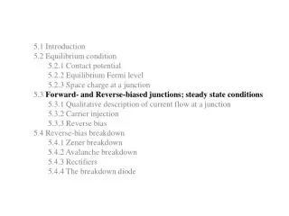
5.1 Introduction 5.2 Equilibrium condition 5.2.1 Contact potential 5.2.2 Equilibrium Fermi level 5.2.3 Space charge at a junction 5.3 Forward- and Reverse-biased junctions; steady state conditions 5.3.1 Qualitative description of current flow at a junction 5.3.2 Carrier injection

E N D
5.1 Introduction • 5.2 Equilibrium condition • 5.2.1 Contact potential • 5.2.2 Equilibrium Fermi level • 5.2.3 Space charge at a junction • 5.3 Forward- and Reverse-biased junctions; steady state conditions • 5.3.1 Qualitative description of current flow at a junction • 5.3.2 Carrier injection • 5.3.3 Reverse bias • 5.4 Reverse-bias breakdown • 5.4.1 Zener breakdown • 5.4.2 Avalanche breakdown • 5.4.3 Rectifiers • 5.4.4 The breakdown diode
For almost all calculations it is valid to assume that an applied voltage appears entirely across the transition region and not in the neutral n and p regions.
The drift current is relatively insensitive to the height of the potential barrier. • The drift current is limited not by how fast carriers are swept down the barrier, but rather how often. • The drift current is not sensitive to electric field, as we normally think.
Forward-biased junction: (a) minority carrier distributions on the two sides of the transition region and definitions of distances Xn and Xp measured from the transition region edges; (b) variation of the quasi-Fermi levels with position.
Example 5-3 Find an expression for the electron current in the n-type material of a forward-biased p-n junction.
5.1 Introduction • 5.2 Equilibrium condition • 5.2.1 Contact potential • 5.2.2 Equilibrium Fermi level • 5.2.3 Space charge at a junction • 5.3 Forward- and Reverse-biased junctions; steady state conditions • 5.3.1 Qualitative description of current flow at a junction • 5.3.2 Carrier injection • 5.3.3 Reverse bias • 5.4 Reverse-bias breakdown • 5.4.1 Zener breakdown • 5.4.2 Avalanche breakdown • 5.4.3 Rectifiers • 5.4.4 The breakdown diode
For Zener breakdown (tunneling) • Extends only a very short distance W from each side of the junction • The metallurgical junction be sharp • The doping high • The tunneling distance d may be too large for appreciable tunneling. However, • d becomes smaller as the reverse bias is increased, because the higher electric fields result in steeper slopes for the band edges • This assumes that the transition region width W does not increase appreciably with reverse bias • For low voltages and heavy doping on each side of the junction, this is a good assumption • If Zener breakdown does not occur with reverse bias of a few volts, avalanche breakdown will become dominant
For Avalanche breakdown • Impact ionization rather than field ionization (Zener) • Carrier multiplication • The peak electric field within W increases with increased doping on the more lightly doped side of the junction (from Eq. 5-23b and Eq. 5-17)
Example 5-4 An abrupt Si p-n junction (A=10-4 cm2) has the following properties at 300 K: The junction is forward biased by 0.5 v. What is the forward current? What is the current at a reverse bias of -0.5 V?
Consideration for rectifier • Junction diodes designed for use as rectifiers should have I-V characteristics as close as possible to that of the ideal diode. • The reverse current should be negligible • The forward current should exhibit little voltage dependence (negligible forward resistance R) • The reverse breakdown voltage should be large • The offset voltage Eo in the forward direction should be small. • Large bandgap • small ni • Small reverse saturation current • Operable at high temperature • Reduced thermal excited EHPs • Increased contact potential • Increased offset voltage Eo
Consideration of doping concentration • The doping concentration on each side of the junction influences the avalanche breakdown voltage, the contact potential, and the series resistance of the diode. • For p+-n junction, the lightly doped region determines many of the properties of the junction. • High-resistivity region should be used for at least one side of the junction to increase the breakdown voltage Vbr. • However, this approach tends to increase the forward resistance R • Contribute to resistant heating • Countermeasure • make large area of the lightly doped region • The lightly doped region of the junction cannot be made arbitrarily short for punch-through.
Avoid premature breakdown across the edge • Beveling • Guard ring
Consideration of p+-n-n+ structure • In fabricating a p+-n or p+-n junction, • It is common to terminate the lightly doped region with a heavily doped layer of the same type for ohmic contact to the device • The result is a p+-n-n+ structure with the p+-n layer serving as the active junction • The lightly doped center region determines the avalanche breakdown voltage • If this region is short compared with the minority carrier diffusion length, the excess carrier injection for large forward currents can increase the conductivity of the region significantly • This type of conductivity modulation, which reduces the forward resistance R, can be very useful for high-current devices • On the other hand, a short, lightly doped center region can also lead to punch-through under reverse bias.
Consideration of Mounting of Rectifier Junction • The mounting of a rectifier junction is critical to its ability to handle power. • For diodes used in low-power circuits, glass or plastic encapsulation or a simple header mounting is adequate. • For high current devices, special mountings to transfer thermal energy away from the junction I s required. • A typical Si power rectifier is mounted on a molybdenum or tungsten disk to match the thermal expansion properties of the Si. • This disk is fastened to a large stud of copper or other thermally conductive material that can be bolted to a heat sink.
5.4.4 The breakdown diode Breakdown Turn-on • Mechanisms for breakdown • The Zener effect (tunneling) breakdown mechanism (field ionization) is for abrupt junctions with extremely heavy doping. • The more common breakdown is avalanche (impact ionization), typically of more lightly doped or graded junctions. • Breakdown material destruction • There is nothing inherently destructive about reverse breakdown. • If current is not limited externally, the junction can be damaged by excess reverse current, through overheat. • the destruction of the device is not necessarily due to mechanisms unique to reverse breakdown.
The voltage regulators • When a diode is designed for a specific breakdown voltage, it is called a breakdown diode. • Such diodes are also called Zener diodes, despite the fact that the actual breakdown mechanism is usually the avalanche effect. • Breakdown diodes can be used as voltage regulators in circuits with varying inputs.
Load line Voltage Drop across the Diode
5.5 Transient and A-C Conditions • 5.5.1 Time Variation of Stored Charges • 5.5.2 Reverse Recovery Transient • 5.5.3 Switching Diodes • 5.5.4 Capacitance of p-n Junctions • 5.5.5 The varactor Diode • 5.6 Deviations from the Simple Theory • 5.6.1 Effect of Contact Potential on Carrier Injection • 5.6.2 Recombination and Generation in the Transition Region • 5.6.3 Ohmic Losses • 5.6.4 Graded Junctions • 5.7 Metal-semiconductor Junctions • 5.7.1 Schottky Barriers • 5.7.2 Rectifying Contacts • 5.7.3 Ohmic Contacts • 5.7.4 Typical Schottky Barriers • 5.8 Heterojunctions
The hole distribution does not remain in the convenient exponential form. • Since the injected hole current is proportional to the gradient of the hole distribution at xn=0, zero current implies zero gradient. • An approximate solution for v(t) can be obtained by assuming an exponential distribution for p at every instant during the decay. • Quasi-steady state approximation
Voltage across a p-n junction cannot be changed instantaneously. 1. 2. The switching process can be made still faster by purposely adding recombination centers, such as Au atoms in Si, to increase the recombination rate.
Example 5-5 Assume a p+-n diode is biased in the forward direction, with a current If. At time t=0 the current is switched to –Ir. Use the appropriate boundary conditions to solve i(t) for Qp(t). Apply the quasi-steady state approximation to find the storage delay time tsd.