Download
1 / 21
210 likes | 233 Vues
Learn about CPLD and FPGA families, programming blocks, interconnect architectures, logic elements, and technology mapping for efficient implementation in digital systems. Understand the spectrum of implementation options from ASIC to reconfigurable hardware. Follow the basic steps such as technology mapping, placement, and routing in FPGA design. Includes examples like logic synthesis, LUT circuits, and full adder implementations.

E N D
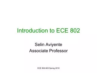
ECE 465Introduction to CPLDs and FPGAs Shantanu Dutt ECE Dept. University of Illinois at Chicago Acknowledgement: Extracted from lecture notes of Dr. Mohamed M. Elkhatib, German University of Cairo and Prof. Russell Tessier, Univ. of Massachusetts. Some modfications and additions done by Prof. Dutt.
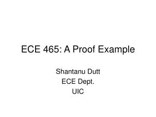
1 0 0 FF FF FF FF FF 1 0 O/Ps I/Ps CPLD Block Diagram An individual switch In a crossbar is a diamond switch Programmable switch for interconnecting various FBs Function block (~ PLA w/ 1 o/p that can be FF’ed) Crossbar Switch
CPLD Function Block Extra function (e.g., g, h) i/ps for OR term 2:1 Mux Example function f= ab+bc’+g+h D-FF PLA-like AND array Literal inputs (e.g., a, b, c)
FPGA Types (Anti-fuse technology)
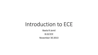
SRAM-type FPGA Interconnect Architecture Diamond switch Horizontal routing (interconnect) channel PSM: Programmable Switch Matrix (for making connections between interconnects of different channels). The structure shown only allows i-to-i connections Vertical routing channels CLB: Configuration Logic Block (programmable logic cell)
SRAM-type FPGA InterconnectArchitecture (contd) Cell Connection Matrix (CCM) PSM
Configuration Logic Block (CLB) • 5-i/p function implemented using G, F and H LUTs (Look Up Tables) using Shannon’s • Expansion: p(a,b,c,d,e) = a p(1, b, c, d, e) + a’ p(0, b, c, d, e) = a q(b,c,d,e) + a’r(b,c,d,e). • q( ) impl. using LUT G, r impl. using LUT F and p=ag + a’h impl. using LUT H • The LUT o/ps can go through a FF (for seq. ckt design) or bypass it for a combinational o/p • This is called technology mapping: mapping the logic to CLB logic components
Digital System: Implementation Spectrum • ASIC gives high performance at cost of inflexibility. • Processor is very flexible but not tuned to the application. • Reconfigurable hardware is a nice compromise. Microprocessor Reconfigurable Hardware ASIC Hardware Software Firmware
High-level Compilers & FPGAs • Difficult to estimate hardware resources. • Some parts of program more appropriate for processor (hardware/software codesign). • Compiler must parallelize computation across many resources. • Engineers like to write in C/VHDL/Verilog rather than pushing little blocks around. for (i = 0; i<n, i++) { c[i] = a[i] + b[i] } Some success stories
RTL . . C = A+B . Array Circuit A + C B Translating a Design to an FPGA • CAD to translate circuit from text description to physical implementation well understood. • Most current FPGA designers use register-transfer level specification (allocation and scheduling) • Same basic steps as ASIC design.
LUT Circuit Compilation & Implementation: Basic Steps • Technology Mapping • Placement • Routing LUT • 4. Convert all implementation “details” to FPGA programming info (configuration bits): LUT RAM bits, CCM & PSM FF/SRAM bits, etc. • Can store config bits on disk or ROM and load into FPGA as needed • Can thus use the FPGA to implement multiple digital systems (at different times or sometimes simultaneously in different FPGA partitions) ? Assign a logical LUT to a physical location. Select wire segments and switches for Interconnection.
A B Co FA Ci S Technology Mapping: A Simple Example Made of Full Adders A+B = D Logic synthesis tool reduces circuit to SOP form S = ABCi + ABCi + ABCi + ABCi A A B B LUT Co LUT S Ci Ci Co = ABCi + ABCi + ABCi + ABCi
Processor + FPGA Three possibilities daughtercard Proc FPGA chip Backplane bus (e.g. PCI) 1. FPGA serves as coprocessor for data intensive applications – possible project. FPGA chip Proc 2. FPGA serves as embedded digital system for lower latency processing. “Reconfigurable Functional Unit”