Chapter 11 Frequency Response
Chapter 11 Frequency Response. 11.1 Fundamental Concepts 11.2 High-Frequency Models of Transistors 11.3 Analysis Procedure 11.4 Frequency Response of CE and CS Stages 11.5 Frequency Response of CB and CG Stages 11.6 Frequency Response of Followers

Chapter 11 Frequency Response
E N D
Presentation Transcript
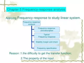
Chapter 11 Frequency Response • 11.1 Fundamental Concepts • 11.2 High-Frequency Models of Transistors • 11.3 Analysis Procedure • 11.4 Frequency Response of CE and CS Stages • 11.5 Frequency Response of CB and CG Stages • 11.6 Frequency Response of Followers • 11.7 Frequency Response of Cascode Stage • 11.8 Frequency Response of Differential Pairs • 11.9 Additional Examples
Chapter Outline CH 11 Frequency Response
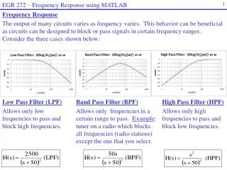
High Frequency Roll-off of Amplifier As frequency of operation increases, the gain of amplifier decreases. This chapter analyzes this problem. CH 11 Frequency Response
Example: Human Voice I Natural Voice Telephone System Natural human voice spans a frequency range from 20Hz to 20KHz, however conventional telephone system passes frequencies from 400Hz to 3.5KHz. Therefore phone conversation differs from face-to-face conversation. CH 11 Frequency Response
Example: Human Voice II Path traveled by the human voice to the voice recorder Mouth Air Recorder Path traveled by the human voice to the human ear Mouth Air Ear Skull • Since the paths are different, the results will also be different. CH 11 Frequency Response
Example: Video Signal High Bandwidth Low Bandwidth Video signals without sufficient bandwidth become fuzzy as they fail to abruptly change the contrast of pictures from complete white into complete black. CH 11 Frequency Response
Gain Roll-off: Simple Low-pass Filter In this simple example, as frequency increases the impedance of C1 decreases and the voltage divider consists of C1 and R1 attenuates Vin to a greater extent at the output. CH 11 Frequency Response
Gain Roll-off: Common Source The capacitive load, CL, is the culprit for gain roll-off since at high frequency, it will “steal” away some signal current and shunt it to ground. CH 11 Frequency Response
Frequency Response of the CS Stage At low frequency, the capacitor is effectively open and the gain is flat. As frequency increases, the capacitor tends to a short and the gain starts to decrease. A special frequency is ω=1/(RDCL), where the gain drops by 3dB. CH 11 Frequency Response
Example: Figure of Merit This metric quantifies a circuit’s gain, bandwidth, and power dissipation. In the bipolar case, low temperature, supply, and load capacitance mark a superior figure of merit. CH 11 Frequency Response
Example: Relationship between Frequency Response and Step Response • The relationship is such that as R1C1 increases, the bandwidth drops and the step response becomes slower. CH 11 Frequency Response
Bode Plot When we hit a zero, ωzj, the Bode magnitude rises with a slope of +20dB/dec. When we hit a pole, ωpj, the Bode magnitude falls with a slope of -20dB/dec CH 11 Frequency Response
Example: Bode Plot The circuit only has one pole (no zero) at 1/(RDCL), so the slope drops from 0 to -20dB/dec as we pass ωp1. CH 11 Frequency Response
Pole Identification Example I CH 11 Frequency Response
Pole Identification Example II CH 11 Frequency Response
Circuit with Floating Capacitor The pole of a circuit is computed by finding the effective resistance and capacitance from a node to GROUND. The circuit above creates a problem since neither terminal of CF is grounded. CH 11 Frequency Response
Miller’s Theorem If Av is the gain from node 1 to 2, then a floating impedance ZF can be converted to two grounded impedances Z1 and Z2. CH 11 Frequency Response
Miller Multiplication With Miller’s theorem, we can separate the floating capacitor. However, the input capacitor is larger than the original floating capacitor. We call this Miller multiplication. CH 11 Frequency Response
Example: Miller Theorem CH 11 Frequency Response
High-Pass Filter Response • The voltage division between a resistor and a capacitor can be configured such that the gain at low frequency is reduced. CH 11 Frequency Response 20
Example: Audio Amplifier • In order to successfully pass audio band frequencies (20 Hz-20 KHz), large input and output capacitances are needed. CH 11 Frequency Response 21
Direct Coupling Capacitive Coupling Capacitive Coupling vs. Direct Coupling • Capacitive coupling, also known as AC coupling, passes AC signals from Y to X while blocking DC contents. • This technique allows independent bias conditions between stages. Direct coupling does not. CH 11 Frequency Response 22
Lower Corner Upper Corner Typical Frequency Response CH 11 Frequency Response 23
High-Frequency Bipolar Model At high frequency, capacitive effects come into play. Cb represents the base charge, whereas C and Cje are the junction capacitances. CH 11 Frequency Response
High-Frequency Model of Integrated Bipolar Transistor Since an integrated bipolar circuit is fabricated on top of a substrate, another junction capacitance exists between the collector and substrate, namely CCS. CH 11 Frequency Response
Example: Capacitance Identification CH 11 Frequency Response
MOS Intrinsic Capacitances For a MOS, there exist oxide capacitance from gate to channel, junction capacitances from source/drain to substrate, and overlap capacitance from gate to source/drain. CH 11 Frequency Response
Gate Oxide Capacitance Partition and Full Model The gate oxide capacitance is often partitioned between source and drain. In saturation, C2~ Cgate, and C1 ~ 0. They are in parallel with the overlap capacitance to form CGS and CGD. CH 11 Frequency Response
Example: Capacitance Identification CH 11 Frequency Response
Transit Frequency Transit frequency, fT, is defined as the frequency where the current gain from input to output drops to 1. CH 11 Frequency Response
Example: Transit Frequency Calculation CH 11 Frequency Response 31
Analysis Summary • The frequency response refers to the magnitude of the transfer function. • Bode’s approximation simplifies the plotting of the frequency response if poles and zeros are known. • In general, it is possible to associate a pole with each node in the signal path. • Miller’s theorem helps to decompose floating capacitors into grounded elements. • Bipolar and MOS devices exhibit various capacitances that limit the speed of circuits. CH 11 Frequency Response 32
High Frequency Circuit Analysis Procedure • Determine which capacitor impact the low-frequency region of the response and calculate the low-frequency pole (neglect transistor capacitance). • Calculate the midband gain by replacing the capacitors with short circuits (neglect transistor capacitance). • Include transistor capacitances. • Merge capacitors connected to AC grounds and omit those that play no role in the circuit. • Determine the high-frequency poles and zeros. • Plot the frequency response using Bode’s rules or exact analysis. CH 11 Frequency Response 33
Frequency Response of CS Stagewith Bypassed Degeneration • In order to increase the midband gain, a capacitor Cb is placed in parallel with Rs. • The pole frequency must be well below the lowest signal frequency to avoid the effect of degeneration. CH 11 Frequency Response 34
Unified Model for CE and CS Stages CH 11 Frequency Response
Unified Model Using Miller’s Theorem CH 11 Frequency Response
Example: CE Stage • The input pole is the bottleneck for speed. CH 11 Frequency Response 37
Example: Half Width CS Stage CH 11 Frequency Response 38
Direct Analysis of CE and CS Stages Direct analysis yields different pole locations and an extra zero. CH 11 Frequency Response
Example: CE and CS Direct Analysis CH 11 Frequency Response
Example: Comparison Between Different Methods Dominant Pole Exact Miller’s CH 11 Frequency Response 41
Input Impedance of CE and CS Stages CH 11 Frequency Response
Low Frequency Response of CB and CG Stages • As with CE and CS stages, the use of capacitive coupling leads to low-frequency roll-off in CB and CG stages (although a CB stage is shown above, a CG stage is similar). CH 11 Frequency Response 43
Frequency Response of CB Stage CH 11 Frequency Response
Frequency Response of CG Stage Similar to a CB stage, the input pole is on the order of fT, so rarely a speed bottleneck. CH 11 Frequency Response
Example: CG Stage Pole Identification CH 11 Frequency Response
Example: Frequency Response of CG Stage CH 11 Frequency Response
Emitter and Source Followers The following will discuss the frequency response of emitter and source followers using direct analysis. Emitter follower is treated first and source follower is derived easily by allowing r to go to infinity. CH 11 Frequency Response
Direct Analysis of Emitter Follower CH 11 Frequency Response
Direct Analysis of Source Follower Stage CH 11 Frequency Response