
Bulk micromachining
E N D
Presentation Transcript
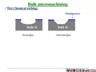
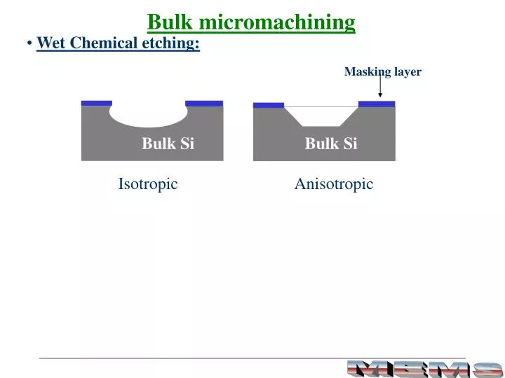
Bulk micromachining • Wet Chemical etching: Masking layer Bulk Si Bulk Si Isotropic Anisotropic
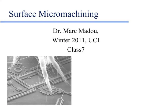
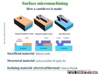
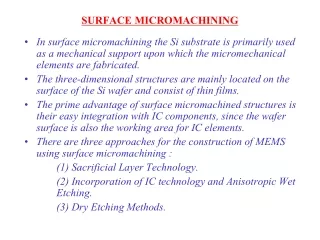
Surface micromachining Carving of layers put down sequentially on the substrate by using selective etching of sacrificial thin films to form free-standing/completely released thin-film microstructures http://www.darpa.mil/mto/mems HF can etch Silicon oxide but does not affect Silicon Release step crucial
MEMS: Foundry services SAMPLES: Sandia Agile MEMS Prototyping, Layout tools, Education and Services (Current process: SUMMIT V) Sandia’s Ultra-planar Multi-level MEMS Technology) - 5 levels of poly-silicon - $10,000 / design MUMPS: Multi-user MEMS processes - Derived from the BSAC processes at U.C. Berkeley - 3-levels of poly-Si
Process steps for fabricating a MEMS device MUMPS: Multi-user MEMS processes > Commercially operated, a repository of processing, design libraries > Standard processing steps, can be custom-designed Poly-MUMPS: Three-layer polysilicon process Metal-MUMPS: Ni electroplating process SOI-MUMPS: Silicon-on-Insulator micromachining process
The CRONOS process for a micro-motor e.g., Synchronous motor Stator Rotor
The CRONOS process for a micro-motor Poly-silicon (POLY): Structural Material Silicon Oxide/PSG (OXIDE): Sacrificial material Silicon Nitride (NITRIDE): for isolation - 8 photo-masks: 8 levels of processing
The cross-sections are depicted in MEMS processing … http://mems.sandia.gov/
Photoresist Photoresist (PR) Photoresist RIE removes POLY0 Photoresist washed away Oxide sacrificial layer deposited by LPCVD PR applied, dimples patterned, and PR washed away (PSG : OXIDE) Oxide patterned and etched, Poly1 deposited
-contd. Pattern POLY1 (4th level), OXIDE & POLY etched: RIE OXIDE 2 Deposit & pattern OXIDE 2, (Level 5) Deposit PR (Level 6) and pattern an ANCHOR contacting POLY 0
- contd. Deposit POLY 2 and OXIDE (PSG) Pattern POLY 2 (7th level) and OXIDE
-contd. Deposit and pattern METAL (Level 8) POLY 2 RELEASE structure, OXIDES are sacrificial STATOR ROTOR STATOR
Case Studies in MEMS Case study Technology Transduction Packaging Pressure sensor Bulk micromach. Piezoresistive sensing Plastic + bipolar circuitry of diaphragm deflection Accelerometer Surface micromach. Capacitive detection of Metal can proof of mass motion Electrostatic Surface micromach. Electrostatic torsion of Glass bonded projection displays + XeF2 release suspended tensile beams Catalytic combustible Surface micromach. Resistance change due Custom mount gas sensor to heat of reaction RF switches Surface micromach. Cantilever actuation Glass bonded DNA amplification Bonded etched glass Pressure driven flow Microcapillaries with PCR across T-controlled zones Lab on a chip Bulk & Surface Electrophoresis & Microfluidics micromachining electrowetting & Polymers
A project on the frontier application areas of MEMS/NEMS Required: A written report + Presentation The project should address the following issues: (1) What is new or novel about this application? (2) Is there any new physical principle being used (3) Where is this headed? (commercial potential, offshoot into new areas of engineering …) (4) Most importantly, YOUR ideas for improvement. Presentations (15 minutes/team of two)
A Piezoresistive Pressure Sensor • Piezoresistance: the variation of electrical resistance with strain • Origin in the deformation of semiconductor energy bands • NOT the same as piezo-electricity • Transduction of stress into voltage • Application: Manifold-Absolute-Pressure (MAP) sensor: Motorola • One of the largest market segments of mechanical MEMS devices
Piezoresistivity Piezoresistive effect is described by a fourth-rank tensor E = re [1 + Π·s] · Jat small strains Electric field Resistivity tensor (2nd rank) Stress Current density
sxx syy szz tyz tzx txy exx eyy ezz gyz gzx gxy sxxtxytxz tyxsyytyz tzxtzyszz exxgxygxz gyxeyygyz gzxgzyezz sij eij ≡ ≡ Tensor notation Stress Strain 4th rank tensor (81 elements) sij = Cijkl ekl From symmetry (no net force in equilibrium) sij = sji 6 independent variables
sxx syy szz tyz tzx txy exx eyy ezz gyz gzx gxy Contracted tensor notation C11 C12 C13 C14 C15 C16 C12 C22 C23 C24 C25 C26 C13 C23 C33 C34 C35 C36 C14 C24 C34 C44 C45 C46 C15 C25 C35 C45 C55 C56 C16 C26 C36 C46 C56 C66 ≡ (6 X 6) matrix, 21 independent elements (as, Cij = Cji)
For cubic materials, e.g. single crystal Silicon, there are only 3 independent constants C11 C12 C12 000 C12 C11 C12 0 0 0 C12 C12 C11 000 0 0 0C44 0 0 0 0 0 0 C44 0 0 0 0 0 0 C44
Piezoresistivity E1 = [1+ p11s1 + p12(s2 + s3)] J1 + p44(t12J2+ t13J3) E2 = [1+ p11s2 + p12(s1 + s3)] J2 + p44(t12J1+ t23J3) E3 = [1+ p11s3 + p12(s1 + s2)] J3 + p44(t13J1+ t23J2) re re re Piezoresistive effect is described by a fourth-rank tensor E = re [1 + Π·s] · J Electric field Resistivity tensor (2nd rank) Stress Current density x 1, y2, z 3, [11, 22, 33, 23, 31, 12] [1, 2, 3, 4, 5, 6] Piezoresistive coefficients rep11 = Π1111 rep12 = Π1122 rep44 = 2Π2323
Longitudinal & transverse piezoresistance DR = plsl + ptstl: longitudinal, t: transverse R Longitudinal & Transverse piezoresistance coefficients • Longitudinal pl Transverse pt • direction direction • (100) p11 (010) p12 • (001) p11 (110) p12 • (111) 1/3 (p11+p12+ 2 p44)(110) 1/3 (p11+2 p12- 2 p44) • (110) 1/2 (p11+p12+ p44) (111) 1/3 (p11+2 p12- p44) • (110) 1/2 (p11+p12+ p44) (001) p44 • (110) 1/2 (p11+p12+ p44) (110) 1/2 (p11 + p12 - p44)
Piezoresistive coefficients of Si - decrease as the doping level/temperature increases C.S. Smith, Phys. Rev. B, vol. 94, pp.42-59, (1954).
Concept of a piezoresistive sensing scheme Max. surface stress Proof Mass Substrate Flexure If piezo-resistor is along [110]: n-type: pl: -31.2 · 10-11 Pa-1, pt: -17.6 · 10-11 Pa-1 p-type: pl: 71.8 · 10-11 Pa-1, pt: -66.3 · 10-11 Pa-1 Transverse Longitudinal - more sensitive - easier to align
R3 R2 + - R1 R4 V DR1 = (pl + npt)sl = (67.6 · 10-11) sl R1 Principle of measurement Diaphragm Poisson ratio, n = 0.06 CROSS-SECTION TOP VIEW DR2 = - (61.7· 10-11) sl R2 R2 WHEATSTONE BRIDGE R3 R1 R4 Vo R1 = R3 = (1+ a1) Ro R2 = R4 = (1 - a2) Ro ai = Σpisi
Support Cantilever Piezoresistors 2 3 wmax Cantilever tip displacement (w) for a point load = 2 d2w x x dx2 1- Lc 3Lc Resistance change due to stress Lc: cantilever length x: distance from support t: thickness x = 3 wmax (Lc - x) Radius of curvature = 1/r = Lc3 [(t/2)/r] = E sl DR = pl sl R Stress = E · Strain
The Motorola MAP sensor http://www.motorola.com/automotive/prod_sensors.html • MAP: Manifold Absolute Pressure • Sensor measures mass airflow into the engine, to control • air-fuel ratio • Uses piezoresistance to measure diaphragm bending with • integrated signal-conditioning and calibration circuitry S. Senturia, page 461, Microsystem design
Al metallization OXIDE n+ - collector n-epi p-type piezoresistor n+ - Emitter p-base <100> p-Si substrate n+ - buried layer Process flow for MAP sensor • Bipolar (NPN) instead of MOS processing on (100) wafers • uses only one piezo-resistor: Xducer
Pressure sensor fabrication and packaging Piezoresistor element DIAPHRAGM Glass frit/Anodic bond