Guide to Surface Micromachining Techniques in MEMS
Learn about surface micromachining in MEMS technology, its advantages, key processing steps, and material systems. Discover the construction methods and applications in this detailed guide.

Guide to Surface Micromachining Techniques in MEMS
E N D
Presentation Transcript
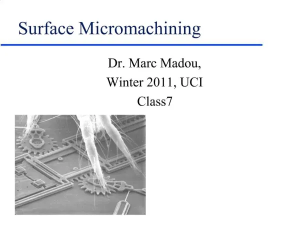
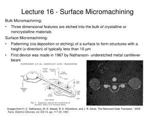
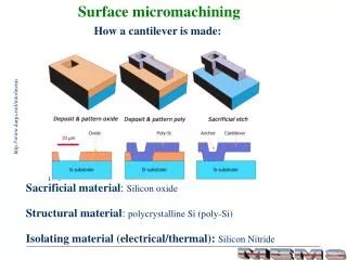
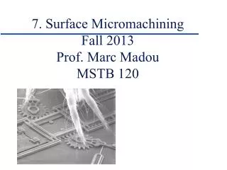
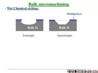
SURFACE MICROMACHINING • In surface micromachining the Si substrate is primarily used as a mechanical support upon which the micromechanical elements are fabricated. • The three-dimensional structures are mainly located on the surface of the Si wafer and consist of thin films. • The prime advantage of surface micromachined structures is their easy integration with IC components, since the wafer surface is also the working area for IC elements. • There are three approaches for the construction of MEMS using surface micromachining : (1) Sacrificial Layer Technology. (2) Incorporation of IC technology and Anisotropic Wet Etching. (3) Dry Etching Methods.
(1) SACRIFICIAL LAYER TECHNOLOGY • In most cases it uses a certain material as the structural material for the fabrication of free-standing structures. • Sacrificial layer technology also utilizes another material as a sacrificial material that is used during processing to realize some specific design requirements, however it does not constitute any part of the final device. • The key processing steps are : (i) Deposition and patterning of the sacrificial layer on substrate. (ii) Deposition and definition of the structural layer. (iii) Removal of the sacrificial layer by lateral etching.
Processes With One Sacrificial Layer and One Structural Layer Take the example of a cantilever : (1) Simple Process
Surface Micromachining Material Systems • Surface micromachining requires a compatible set of structural materials, sacrificial materials and chemical etchants. • The structural materials must possess the physical and chemical properties that are suitable for the desired application. In addition, the structural materials must have satisfactory mechanical properties ; e. g., high yield and fracture stresses, minimal creep and fatigue, good wear resistance. • The sacrificial materials must also have good mechanical properties to avoid device failure during fabrication. These properties include good adhesion and low residual stresses in order to eliminate device failure by delamination and/or cracking. • The etchants must have excellent etch selectivity and they must be able to etch off the sacrificial materials without affecting the structural ones. The etchants must have proper viscosity and surface tension characteristics.
(1) Poly-Si/Silicon Dioxide • This is the most common material system : LPCVD deposited poly-Si as the structural material and thermally grown or LPCVD deposited oxide as the sacrificial material. • The oxide is readily dissolved in HF without the poly-Si being affected. • Advantages : • - Both materials are used in IC processing and, therefore, their deposition technologies are readily available. • - Poly-Si has excellent mechanical properties and can be doped for various electrical applications. • - The oxide can be thermally grown and CVD deposited at a wide temperature range (~ 200 °C to ~ 1200 °C) which is very useful for various processing requirements. • - The material system is compatible with IC processing. • Together with this material system silicon nitride is often used for electrical insulation. Common Material Systems
(2) Silicon Nitride/Poly-Si • Here LPCVD silicon nitride is used as the structural material, whereas poly-Si is the sacrificial material. • In this case Si anisotropic etchants such as KOH and EDP are used to dissolve poly-Si. • (3) Tungsten/Silicon Dioxide • CVD deposited tungsten is used as the structural material with the oxide as the sacrificial material. • HF is used for removing the oxide.
(4) Polyimide/Aluminum • Polyimide is the structural material and aluminum is the sacrificial material. • Acid-based aluminum etchants are used to dissolve the aluminum sacrificial material. • Advantages : • - Polyimide has a small elastic modulus which is ~ 50 times smaller than that of poly-Si. • - Polyimide can take large strains before fracture. • - Both polyimide and aluminum can be prepared at low temperatures (< 400 °C). • A disadvantage of polyimide is its viscoelastic characteristics; it creeps.
Processes With Two Sacrificial Layers and Two Structural Layers Take the example of a rotor : (i) Center-Pin Bearing
The 2+1/2 Polysilicon Process • The 2+1/2 poly process requires three poly-Si depositions, two silicon dioxide depositions and one silicon nitride deposition along with six patterning steps. • We take the example of a center-pin side-drive micromotor. - Variable-capacitance side-drive micromotors require electrically conducting materials for the rotor and the stator; this is satisfied by heavily P-doped poly-Si. - The stator poles need to be electrically isolated from the rotor, the substrate, and one another; LPCVD silicon nitride will do this job.
Side-drive micromotor : Process Flow