Download
1 / 45
450 likes | 609 Vues
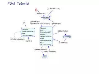
This document explores the principles of Finite State Machines (FSM), focusing on their design and optimization in digital circuits. It outlines the characteristics of combinational and sequential circuits, detailing synchronous and asynchronous FSMs. The Mealy and Moore models are discussed, highlighting their components and applications. The guide includes FSM design steps such as understanding specifications, state representation, minimization, and state assignments using a vending machine example. Key optimization techniques and the transition functions are also covered, providing a robust understanding of FSM implementation in FPGA-based systems.

E N D
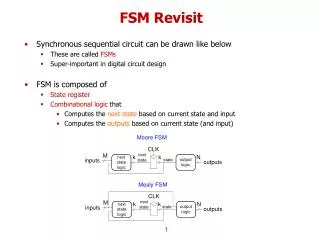
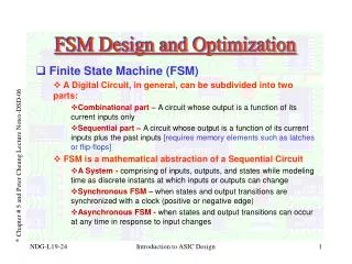
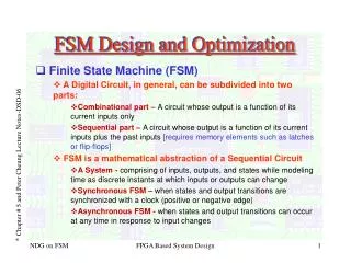
FSM Design and Optimization • Finite State Machine (FSM) • A Digital Circuit, in general, can be subdivided into two parts: • Combinational part – A circuit whose output is a function of its current inputs only • Sequential part – A circuit whose output is a function of its current inputs plus the past inputs [requires memory elements such as latches or flip-flops] • FSM is a mathematical abstraction of a Sequential Circuit • A System - comprising of inputs, outputs, and states while modeling time as discrete instants at which inputs or outputs can change • Synchronous FSM – when states and output transitions are synchronized with a clock (positive or negative edge) • Asynchronous FSM - when states and output transitions can occur at any time in response to input changes * Chapter # 5 and Peter Cheung Lecture Notes-DSD-06 FPGA Based System Design
FSM Design and Optimization • FSM Models • Mealy Model – Contains three components: • State Memory to store the current state S(t) • State Transition Function to determine the next state S(t+1) depending upon the current state S(t) and the input X(t) • Output Function which generates the output Y(t) as function of the current state S(t) and the input X(t) * Chapter # 5 and Peter Cheung Lecture Notes-DSD-06 Fig-01: Mealy Model of FSM FPGA Based System Design
FSM Design and Optimization • FSM Models – Cont’d • Moore Model –Similar to Mealy Model except thatOutput Function which generates the output Y(t) as function of the current state S(t) only. • Both Mealy and Moore Models can be mapped into each other • Mealy Machines usually have fewer state variables (memory elements)- Widely used in Engineering Applications • Moore Machines are simpler to analyze mathematically * Chapter # 5 and Peter Cheung Lecture Notes-DSD-06 Fig-02: Moore Model of FSM FPGA Based System Design
FSM Design and Optimization • FSM Models – Cont’d • A Problem with Mealy Machine (as shown in Fig-01) – Output may have glitches. So, a slightly modified version of Mealy Machine is more commonly used. * Chapter # 5 and Peter Cheung Lecture Notes-DSD-06 Fig-03: Mealy FSM with Registered Output • All Digital Systems can be viewed as networks of FSMs ? FPGA Based System Design
FSM Design and Optimization • FSM Models – Cont’d • Autonomous FSM – Special FSM having no inputs, e.g. LFSR • Communicating FSMs – Two or more FSMs interacting with each other * Chapter # 5 and Peter Cheung Lecture Notes-DSD-06 Fig-04: Communicating FSMs FPGA Based System Design
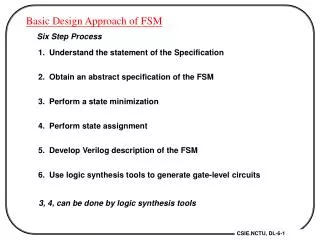
FSM Design and Optimization • FSM Design Steps • Understand the Specifications • Problem Definition Using State Diagram and/or State Table • State Minimization – Removal of redundant internal states • State Assignment – Assigning binary codes to the states • Determination of State Transition Function and Output Function Equations • Logic Equation Minimization • Design Mapping to a given Technology or Device • Steps 3, 4 and 6 are Optimization Problems –valuable but not necessary steps * Chapter # 5 and Peter Cheung Lecture Notes-DSD-06 FPGA Based System Design
FSM Design and Optimization • FSM Design Steps – Cont’d • Step-1: Understanding the Specifications A Simple Vending Machine Design Example: [a] Accepts 1 or 2 Rupees Coins [b] Delivers a Pak-Cola bottle of drink costing Rupees 3 [c] Provides change where applicable * Chapter # 5 and Peter Cheung Lecture Notes-DSD-06 Fig-05: A Vending Machine Model FPGA Based System Design
FSM Design and Optimization • FSM Design Steps – Cont’d • Step-2: State Diagram Representation • Each State is represented as a circle with output arrows • Next to the arrow, input and outputs are given • For Vending Machine, FSM remains in state S0 until there is some coin, either of Rs. 1 or Rs. 2 inserted. • Upon such an event, depending upon the coin type, it switches to another state • FSM should not activate the Vend / Change driver unless the credit equals or exceed the Rs. 3 • A state transition diagram can be drawn as shown in Fig-07(Next Slide) * Chapter # 5 and Peter Cheung Lecture Notes-DSD-06 Fig-06: Notation used in State Diagram Representation FPGA Based System Design
FSM Design and Optimization • FSM Design Steps – Cont’d • Step-2: State Diagram Representation – Let us Complete it Inputs/Outputs = Rs.2:Rs.1/Vend:Change * Chapter # 5 and Peter Cheung Lecture Notes-DSD-06 Fig-07: State Diagram Representation of Vending Machine FPGA Based System Design
[a] [b] FSM Design and Optimization • FSM Design Steps – Cont’d • Step-3: State Minimization Equivalent States: Two states are said to be equivalent if they have identical next states and outputs. * Chapter # 5 and Peter Cheung Lecture Notes-DSD-06 Fig-08: State Minimization Step-03 [a] Cyclic State Diagram of VM [b] Reduced FSM for VM FPGA Based System Design
FSM Design and Optimization • FSM Design Steps – Cont’d • Step-3: State Minimization – Cont’d • Addition of Invalid State(s) due to State Assignment (Binary Codes) * Chapter # 5 and Peter Cheung Lecture Notes-DSD-06 Fig-09: Final Reduced FSM for VM FPGA Based System Design
FSM Design and Optimization • FSM Design Steps – Cont’d Step-4: State Assignment and State Transition Table * Chapter # 5 and Peter Cheung Lecture Notes-DSD-06 FPGA Based System Design
FSM Design and Optimization • FSM Design Steps – Cont’d Step-4: State Assignment and State Transition Table • Step-5: Determination of Logical Equations * Chapter # 5 and Peter Cheung Lecture Notes-DSD-06 ? FPGA Based System Design
FSM Design and Optimization • FSM Design Steps – Cont’d • Step-6-7: Simplification of Logic Equations and Hardware Implementation • Use of K Maps or Other Methods • Implementation is Technology Dependent * Chapter # 5 and Peter Cheung Lecture Notes-DSD-06 Fig-10: Implementation of VM FSM FPGA Based System Design
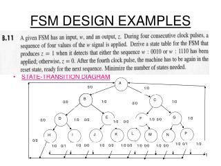
FSM Design and Optimization • FSM Design Example – Huffman Codec • Used for JPEG/MPEG Compression • Relies on known probability of a set of fixed symbols * Chapter # 5 and Peter Cheung Lecture Notes-DSD-06 Table-04: Symbols with Their Binary Code and Frequency Fig-11: Huffman Tree Developed based on Symbol Frequency FPGA Based System Design
FSM Design and Optimization • FSM Design Example – Huffman Codec – Cont’d • Huffman Decoder Circuit Implementation as FSM * Chapter # 5 and Peter Cheung Lecture Notes-DSD-06 Fig-11: Huffman Decoder FSM State Diagram and FSM Implementation FPGA Based System Design
FSM Design and Optimization • FSM Optimization • Three Ways to Optimize the HW Complexity of FSM • State Minimization • State Assignment • Logic Equation Minimization • State Minimization Methods • State Merging by Observation • State Partitioning • Application of Implication Tables • State Merging by Observation • Vending Machine Example • Bit Sequence Detector * Chapter # 5 and Peter Cheung Lecture Notes-DSD-06 FPGA Based System Design
FSM Design and Optimization • FSM Optimization – Cont’d • State Merging by Observation • Bit Sequence Detector – A Circuit that generates an output Z = 1 when it detects a bit sequence from a serial data input D as 001, 010, 100, or 111. • S3 and S6 are Equivalent, and so are S4 and S5. Eliminate S5 and S6 * Chapter # 5 and Peter Cheung Lecture Notes-DSD-06 Fig-12: Bit Sequence Detector [a] State Diagram [b] State Table FPGA Based System Design
FSM Design and Optimization • FSM Optimization – Cont’d • State Merging by Observation – Cont’d • Bit Sequence Detector after State Minimization * Chapter # 5 and Peter Cheung Lecture Notes-DSD-06 Fig-13: Minimal State Bit Sequence Detector [a] Stat Table [b] State Diagram State Partitioning FPGA Based System Design
FSM Design and Optimization • FSM Optimization – Cont’d • State Partitioning • An FSM Example • Best Solution for this FSM takes only 5 States? Fig- 14: State Table for FSM of State Partitioning Example * Chapter # 5 and Peter Cheung Lecture Notes-DSD-06 FPGA Based System Design
FSM Design and Optimization • FSM Optimization – Cont’d • State Partitioning – Cont’d • An FSM Example • Step-1: State Partitioning by Outputs – Divide the states into sets with identical outputs • Step-2: State Partitioning with Next States – For states in each set, find their next states separately * Chapter # 5 and Peter Cheung Lecture Notes-DSD-06 FPGA Based System Design
FSM Design and Optimization • FSM Optimization – Cont’d • State Partitioning – Cont’d • An FSM Example • Step-3: Repartitioning based on Next States – After Step-2, two things have happened: next state group for C (input = 0) now belongs to B2, however, next state group for A (input = 1) now belongs to no single state group, so, A partition has become invalid * Chapter # 5 and Peter Cheung Lecture Notes-DSD-06 NOW all the next state groupings belong to some single state partition/group. WHAT is Final Partitioning? FPGA Based System Design
FSM Design and Optimization • FSM Optimization – Cont’d • State Partitioning – Cont’d • An FSM Example • Finally We got a State Partitioning Where Next outputs are the same for each state in the same state partition/group AND Next states are the same for each state in the same set/group * Chapter # 5 and Peter Cheung Lecture Notes-DSD-06 Final Optimized FSM has got only Five States……………….! FPGA Based System Design
FSM Design and Optimization • FSM Optimization – Cont’d Self-study Exercise:Application of Implication Table: Easy to Computerize and Suitable for Larger FSM Optimization * Chapter # 5 and Peter Cheung Lecture Notes-DSD-06 State Assignment ASM Chart FSM Synthesis Next Week: FPGA Based System Design
FSM Design and Optimization • FSM Optimization – Cont’d • State Assignment • Assigning Unique Binary Codes to the States of a Minimized FSM • State Minimization has a Unique Technology-Independent Solution, however, State Assignment Depends on • Technology such as PLA, ROM, PAL, logic gates • Type of storage circuit, D-latches or FF • For a FSM of r Rows (States), with n-bit State Variables, All Possible Permutations are N = 2n ! / (2n-r)! • Many, among above Assignments, are just Rearrangements, according to McCluskey, Number of Distinct Assignments is Reduced to ND = (2n -1)! / (2n-r)!* n! * Chapter # 5 and Peter Cheung Lecture Notes-DSD-06 FPGA Based System Design
FSM Design and Optimization • FSM Optimization – Cont’d • State Assignment – Cont’d • Even the number given by McCluskey is still very large • Very Complex Problem, called Intractable or np-Complete. Such a problem usually have no optimal solution but some solution based on heuristics (thumb rules or simple rules) • Aim here would be to have Rules that provide maximum number of 1’s in adjacent cells of next-state truth table for better k-map reduction * Chapter # 5 and Peter Cheung Lecture Notes-DSD-06 FPGA Based System Design
FSM Design and Optimization • FSM Optimization – Cont’d • State Assignment – Cont’d • Rule-1: States with the same next state for a given input condition should be assigned codes differing in one (binary) bit position only. For Example, • Rule-2: Next States of a single state should be given logically adjacent state assignments. For Example, * Chapter # 5 and Peter Cheung Lecture Notes-DSD-06 FPGA Based System Design
FSM Design and Optimization • FSM Optimization – Cont’d • State Assignment – Cont’d Example-01: Consider the Bit Sequence Detector FSM • Applying Rule 2, S1 and S2 should be assigned logically adjacent codes, so, let S1 = 100 and S2 = 101 • Applying Rule 1, S3 and S4 both have the same next state with given input condition, so, S3 and S4 are assigned logically adjacent codes. S3 = 110 and S4 = 111 • S0 can be assigned 000 (arbitrary), and unassigned states would be 010, 011, and 001 * Chapter # 5 and Peter Cheung Lecture Notes-DSD-06 Fig-15: Bit Sequence Detector FSM FPGA Based System Design
FSM Design and Optimization • FSM Optimization – Cont’d • State Assignment – Cont’d • One-Hot State Assignment • Sometimes, instead of log2 r bi-stable latches, it is more efficient (and convenient as well ) to have r latches/flip-flops, i.e. one for each state. It is called One-Hot State Assignment. • At any time, only one FF will be set (FF corresponding to the state where FSM lies at that instant) • No State Assignment is required • One-hot state assignment is particularly suitable for FPGA (LUT and MUX based Architecture) implementation of FSM • Number of FF required is much higher than Min. Length State Encoding • Slower in Operation as compared to other option. * Chapter # 5 and Peter Cheung Lecture Notes-DSD-06 FPGA Based System Design
FSM Design and Optimization • FSM Implementation- HW Considerations • Implementation Alternatives • Standard ICs – Suitable for Simple Designs • PROM –Suitable for many Outputs/States, No Logic Minimization needed, Exhaustive Implementation for all Possible Input Combinations, Size grows Exponentially • CPLDs/FPGAs –More Suitable for most of FSM Implementations Fig-16: Generic Block Diagram of FSM * Chapter # 5 and Peter Cheung Lecture Notes-DSD-06 Fig-17: Implementation of FSM with PROM FPGA Based System Design
FSM Design and Optimization • FSM Implementation- HW Considerations – Cont’d • Asynchronous Inputs – A Possible Source of Race Condition • Asynchronous input “A” to FSM, while making transition from “0” to “1”, as shown above may give rise to a wrong state transition • SOLUTION: Synchronize all the Asynchronous Inputs to FSM using a Latch clocked by the FSM clock Fig-18: Asynchronous Inputs to FSM * Chapter # 5 and Peter Cheung Lecture Notes-DSD-06 Fig-19: Synchronizing Asynchronous Inputs FPGA Based System Design
FSM Design and Optimization • FSM Implementation- HW Considerations – Cont’d • Types of Flip-Flops at Output • Outputs of Programmable Macro-Cells or LEs of CPLDs/FPGAs are Configurable • Inverting/Non-Inverting • Register or Combinational • D Flip-Flop, S-R FF, J-K FF, or T-FF, any type is Possible • T-FF or J-K FF can Produce more Efficient Implementation (fewer product terms in Boolean Equations) • Better CAD toolsmake better choice automatically * Chapter # 5 and Peter Cheung Lecture Notes-DSD-06 FPGA Based System Design
[a] [b] FSM Design and Optimization • Algorithmic State Machine (ASM) Chart • An Alternative Method to Represent FSM based on Flow-Chart Notation – Popularized by Christopher Clare “ Designing Logic Systems Using State Machines” Key Features of ASM: • FSM is in one State Block per state time (Clock Cycle) • Single Entry Point for each State Block • For each combination of inputs, only one unambiguous exit path • Outputs asserted high, low, high-impedance until the next clock cycle * Chapter # 5 and Peter Cheung Lecture Notes-DSD-06 Fig-20: ASM Chart [a] ASM Elements [b] An ASM Block FPGA Based System Design
FSM Design and Optimization • Algorithmic State Machine (ASM) Chart – Cont’d • ASM Construction Rules Must Follow these Rules: • Each State can have one and only one State Box • Outputs depending on the Current State only (Moore Model) are represented by Square Box • Outputs depending on the Inputs (and of course the Current State), as in Mealy Model, are represented by Rounded Box • Decision Box contains the Conditions for the Input Variables * Chapter # 5 and Peter Cheung Lecture Notes-DSD-06 Fig-21: ASM Multi-Way Decision Block Simplification FPGA Based System Design
FSM Design and Optimization • Algorithmic State Machine (ASM) Chart – Cont’d • ASM Advantages over (Bubble) State Diagram • ASM Chart reflects HW Algorithm better than (Bubble) State Diagram Representation of FSM • Easier to Follow and Understand • ASM Chart avoids Transition Conflicts that could Occur in State Diagram Representation of FSM EXAMPLE: Inputs I3I2I1I0 = 1101, 1011, and 1111 all will make both transitions to be True. * Chapter # 5 and Peter Cheung Lecture Notes-DSD-06 Fig-22: Possible Conflicts in State Diagram Representation of an FSM FPGA Based System Design
Rs.0 Rs.2 Rs.2 Rs.1 Rs.1 Rs.2 Rs.1 Rs.1 Rs.2 FSM Design and Optimization • Algorithmic State Machine (ASM) Chart – Cont’d • ASM Representation of Vending Machine * Chapter # 5 and Peter Cheung Lecture Notes-DSD-06 [a] [b] Fig-23: Mealy Model of Vending Machine [a] State Diagram [b] ASM Chart FPGA Based System Design
FSM Design and Optimization • FSM Design Using Verilog HDL • Mealy FSM and Its RTL Coding Fig-24: Mealy FSM to be Coded in Verilog HDL * Chapter # 5 and Peter Cheung Lecture Notes-DSD-06 FPGA Based System Design
FSM Design and Optimization • FSM Design Using Verilog HDL – Cont’d • Mealy FSM and Its RTL Coding – Cont’d * Chapter # 5 and Peter Cheung Lecture Notes-DSD-06 …Cont’d on Next Slide FPGA Based System Design
FSM Design and Optimization • FSM Design Using Verilog HDL – Cont’d • Mealy FSM and Its RTL Coding – Cont’d …Cont’d from Prev. Slide * Chapter # 5 and Peter Cheung Lecture Notes-DSD-06 …Cont’d on Next Slide FPGA Based System Design
FSM Design and Optimization • FSM Design Using Verilog HDL – Cont’d • Mealy FSM and Its RTL Coding – Cont’d …Cont’d from Prev. Slide * Chapter # 5 and Peter Cheung Lecture Notes-DSD-06 …Cont’d on Next Slide FPGA Based System Design
FSM Design and Optimization • FSM Design Using Verilog HDL – Cont’d • Mealy FSM and Its RTL Coding – Cont’d …Cont’d from Prev. Slide * Chapter # 5 and Peter Cheung Lecture Notes-DSD-06 FPGA Based System Design
FSM Design and Optimization • FSM Design Using Verilog HDL – Cont’d • Moore FSM and Its RTL Coding * Chapter # 5 and Peter Cheung Lecture Notes-DSD-06 …Cont’d on Next Slide FPGA Based System Design
FSM Design and Optimization • FSM Design Using Verilog HDL – Cont’d • Moore FSM and Its RTL Coding …Cont’d from Prev. Slide * Chapter # 5 and Peter Cheung Lecture Notes-DSD-06 …Cont’d on Next Slide FPGA Based System Design
FSM Design and Optimization • FSM Design Using Verilog HDL – Cont’d • Moore FSM and Its RTL Coding …Cont’d from Prev. Slide * Chapter # 5 and Peter Cheung Lecture Notes-DSD-06 …Cont’d on Next Slide FPGA Based System Design
FSM Design and Optimization • FSM Design Using Verilog HDL – Cont’d • Moore FSM and Its RTL Coding …Cont’d from Prev. Slide * Chapter # 5 and Peter Cheung Lecture Notes-DSD-06 FPGA Based System Design