Download
1 / 22
570 likes | 2.04k Vues
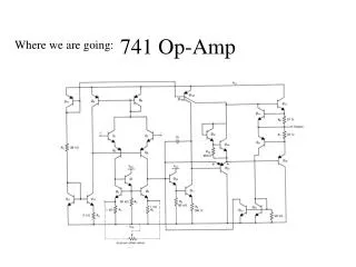
741 Op-Amp Circuit . Section 8.1 ( Razavi ) Chapter 12 ( Sedra Smith). History. The first uA741 Op-Amp was designed by Bob Widlar in 1963 at Fairchild Semidconductor . uA702 sold for 300 a piece. uA709 was sold for 70 a piece.

E N D
741 Op-Amp Circuit Section 8.1 (Razavi) Chapter 12 (Sedra Smith)
History • The first uA741 Op-Amp was designed by Bob Widlar in 1963 at Fairchild Semidconductor. • uA702 sold for 300 a piece. • uA709 was sold for 70 a piece. • Bob asked for a raise, didn’t get it, so he quit. Bob sent to National Semiconductor. • LM101 http://en.wikipedia.org/wiki/Bob_Widlar
History • David Fullagar (Fairchild) • Scrutinize LM 101 • Incorporated a 30 pF Cap. • uA741 was introduced. • Gordon Moore
BJT Op-Amp Input-Stage Bias Reference Bias Current Second-Stage Input-Stage Output-Stage
Reference Bias Current VCC=15 V VEE=-15 V VBE11=0.7 V VEB12=0.7 V IREF=0.73 mA
Input-Stage Bias IREF=0.73 mA R4=5 KΩ (IS10=IS11, assumption) Solve through trial and error IC10=19 uA
Input Stage (1) From previous Calculation: IC10=19 uA (from symmetry) (β is high ) (~0)
Negative Feedback (2) (3) (1) (4) (constant)
Input Stage (3) (IB1) (IB2) (Input Bias Current) (Input Offset Current)
Input Resistance (1) (AC Ground)
Input Resistance (AC Ground) R into the emitter of Q3: 1/gm3 R into the base of Q1: rπ1+β1/gm3 Differential resistance 2(rπ1+β1/gm3) gm=IC/VT Large input resistance since IC is kept small! Typical input impedance is in excess of 2 MOhms
Second-Stage Bias 0.75IS12=IS13B IC12=0.73 mA IC13B=0.55 mA IC17=IC13B (0)
Output Stage Bias (0) IS13,A=0.25IS12 IC23=0.25IREF Assume VBE18=VBE19=0.6 V Βp=50 Βn=200 ICE23=180 uA IR10=15 uA IE18=IE23-IR10 IB18=IC18/200=0.8 uA IE19=IB18+IR10 VBB=VBE18+VBE19 (Output resistance is small) (0)
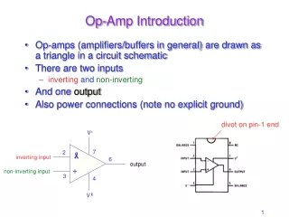
Equivalent Circuit of an Op-Amp Characteristics: Negligible input current Large input AC resistance Small AC output resistanceLarge Voltage Gain
Op-Amp as an Amplifier (non-inverting input) (inverting input) Op-Amp is a circuit that amplifies the difference between the inputs.
Consequence of Large Gain As Ao approaches infinity, Vin1-Vin2 approaches 0.
Unity Gain Buffer (If A0 is 1000, Vout/Vin=0.999)