Zero-voltage transition converters The phase-shifted full bridge converter
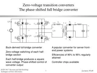
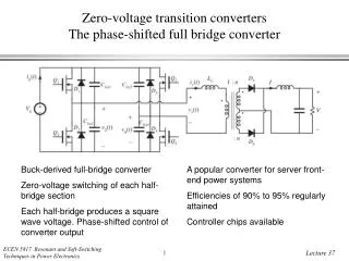
Zero-voltage transition converters The phase-shifted full bridge converter. Buck-derived full-bridge converter Zero-voltage switching of each half-bridge section Each half-bridge produces a square wave voltage. Phase-shifted control of converter output.

Zero-voltage transition converters The phase-shifted full bridge converter
E N D
Presentation Transcript
Zero-voltage transition convertersThe phase-shifted full bridge converter Buck-derived full-bridge converter Zero-voltage switching of each half-bridge section Each half-bridge produces a square wave voltage. Phase-shifted control of converter output A popular converter for server front-end power systems Efficiencies of 90% to 95% regularly attained Controller chips available
Issues with this converter It’s a good converter for many applications requiring isolation. But… • Secondary-side diodes operate with zero-current switching. They require snubbing or other protection to avoid failure associated with avalanche breakdown • The resonant transitions reduce the effective duty cycle and conversion ratio. To compensate, the transformer turns ratio must be increased, leading to increased reflected load current in the primary-side elements • During the D’Ts interval when both output diodes conduct, inductor Lc stores energy (needed for ZVS to initiate the next DTs interval) and its current circulates around the primary-side elements—causing conduction loss
Issues with this converter It’s a good converter for many applications requiring isolation. But… • Secondary-side diodes operate with zero-current switching. They require snubbing or other protection to avoid failure associated with avalanche breakdown • The resonant transitions reduce the effective duty cycle and conversion ratio. To compensate, the transformer turns ratio must be increased, leading to increased reflected load current in the primary-side elements • During the D’Ts interval when both output diodes conduct, inductor Lc stores energy (needed for ZVS to initiate the next DTs interval) and its current circulates around the primary-side elements—causing conduction loss
Approaches to snub the diode ringing(a) conventional diode snubber
Approaches to snub the diode ringing(b) conventional passive voltage-clamp snubber
Approaches to snub the diode ringing(c) simplify to one passive voltage-clamp snubber
Approaches to snub the diode ringing(d) improvement of efficiency in voltage-clamp snubber
Approaches to snub the diode ringing(e) active clamp lossless snubber
Approaches to snub the diode ringing(f) primary-side lossless voltage clamp
PFC DC-DC Load Load Load Another application of the ZVT: DC Transformer Operate at a fixed conversion ratio with high duty cycle, leading to high efficiency—avoids the problems of circulating currents Use other elements in the system to regulate voltage 5 V 1 V 350 V ZVT AC line DC-DC isolation DC-DC
Active clamp circuits • Can be viewed as a lossless voltage-clamp snubber that employs a current-bidirectional switch • See Vinciarelli patent (1982) for use in forward converter • Related to other half-bridge ZVS circuits • Can be added to the transistor in any PWM converter • Not only adds ZVS to forward converter, but also resets transformer better, leading to better transistor utilization than conventional reset circuit
The conventional forward converter • Max vds = 2Vg + ringing • Limited to D < 0.5 • On-state transistor current is P/DVg • Magnetizing current must operate in DCM • Peak transistor voltage occurs during transformer reset • Could reset the transformer with less voltage if interval 3 were reduced
The active-clamp forward converter • Better transistor/transformer utilization • ZVS • Not limited to D < 0.5 Transistors are driven in usual half-bridge manner:
Approximate analysis:ignore resonant transitions, dead times, and resonant elements
Charge balance Vb can be viewed as a flyback converter output. By use of a current-bidirectional switch, there is no DCM, and LM operates in CCM.
Peak transistor voltage Max vds = Vg + Vb = Vg /D’ which is less than the conventional value of 2 Vg when D > 0.5 This can be used to considerable advantage in practical applications where there is a specified range of Vg
Design example • 270 V ≤ Vg ≤ 350 V • max Pload = P = 200 W • Compare designs using conventional 1:1 reset winding and using active clamp circuit
Conventional case Peak vds = 2Vg + ringing = 700 V + ringing Let’s let max D = 0.5 (at Vg = 270 V), which is optimistic Then min D (at Vg = 350 V) is(0.5)(270)/(350) = 0.3857 The on-state transistor current, neglecting ripple, is given by ig = DnI = Did-on with P = 200 W = Vg ig = DVg id-on So id-on = P/DVg = (200W) / (0.5)(270 V) = 1.5 A
Active clamp case:scenario #1 • Suppose we choose the same turns ratio as in the conventional design. Then the converter operates with the same range of duty cycles, and the on-state transistor current is the same. But the transistor voltage is equal to Vg /D’, and is reduced: • At Vg = 270 V: D = 0.5 peak vds = 540 V • At Vg = 350 V: D = 0.3857 peak vds = 570 V • which is considerably less than 700 V
Active clamp case:scenario #2 • Suppose we operate at a higher duty cycle, say, D = 0.5 at Vg = 350 V. Then the transistor voltage is equal to Vg /D’, and is similar to the conventional design under worst-case conditions: • At Vg = 270 V: D = 0.648 peak vds = 767 V • At Vg = 350 V: D = 0.5 peak vds = 700 V • But we can use a lower turns ratio that leads to lower reflected current in Q1: • id-on = P/DVg = (200W) / (0.5)(350 V) = 1.15 A