Introduction to CPU Design
770 likes | 1.04k Vues
Introduction to CPU Design. Computer Organization & Assembly Language Programming Dr Adnan Gutub aagutub ‘at’ uqu.edu.sa [Adapted from slides of Dr. Kip Irvine: Assembly Language for Intel-Based Computers]

Introduction to CPU Design
E N D
Presentation Transcript
Introduction to CPU Design Computer Organization & Assembly Language Programming Dr Adnan Gutub aagutub ‘at’ uqu.edu.sa [Adapted from slides of Dr. Kip Irvine: Assembly Language for Intel-Based Computers] Most Slides contents have been arranged by Dr Muhamed Mudawar & Dr Aiman El-Maleh from Computer Engineering Dept. at KFUPM
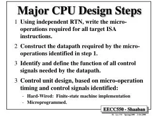
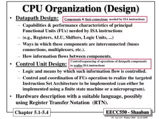
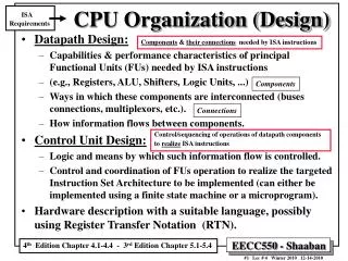
Outline • Introduction • Data Path Design • Register Transfer • Register Transfer Timing • Single Bus CPU Design • Two Bus CPU Design • Three Bus CPU Design • Control Unit Design • Hardwired Control • Microprogrammed Control • Simple CPU Design Example
Introduction • A CPU is decomposed into two main parts: data path & control unit. • Data path consists of registers, arithmetic blocks and interconnections. • The flow of data between registers & arithmetic operations are performed in the data path.
Introduction • Data path is controlled by a set of signals to cause actions to take place. • Examples of such signals are • strobe signals to load registers • signals to control the connectivity of outputs to a bus. • In order to perform an operation on the data path, it is required to generate the control signals in the correct order to affect the correct data path activity. • The control unit receives signals that describe the state of the data path and the control unit sends control signals to the data path.
Register Transfer • The process of instruction execution can be described as a set of register transfer operations. • In each clock, one or more register transfer operations are performed. • Some register transfer operations can’t be implemented in one clock cycle and have to be broken into a number of register transfer operations that have to be performed in a sequence. • Example: ADD AX, BX • 1. Y ← AX • 2. Z ← Y + BX • 3. AX ← Z
Register Transfer • Register transfer A ← B can be implemented by two sets of m flip-flops. • The m-bit data is moved (copied) from register B into register A when the strobe signal is activated. • Assuming rising-edge triggered flip-flops, the transfer operation occurs on the rising edge of the strobe .
Register Transfer • To transfer data between n registers, interconnect registers using n multiplexers. • Input of each register is connected to an (n-1)x1 multiplexer. • In the (n-1)x1 multiplexer, • other n-1 registers are connected to the n-1 inputs of the multiplexer • log (n-1) selection lines are used to select the required register. • Expensive solution with complex routing.
Register Transfer • A better solution is to use a tri-state bus that is shared among all registers. • Registers are connected to the bus through tri-state buffers such that one tri-state buffer is enabled at a time. • Each tri-state buffer is controlled by an output enable signal • when set high connects the input of the buffer to the output • otherwise produces a high-impedance value Z.
Register Transfer • A strobe signal for each register controls register capture • To allow for propagation delay across the bus & FF setup time, registers capture on falling edge of the clock • Tri-state buffer enable signals are activated on rising edge of clock. • This is achieved by Anding the strobe signals with the complement of the clock.
Register Transfer Timing • In a register transfer operation, information is moved out of a register, along a bus, possibly through combinational logic, and into another register. • Tri-state delay: tg • Bus prob. delay: tbp • Combinational delay: tcomb • Setup time & FF prob.: tsu &tff • Minimum Pulse Width • tw = tg + tbp + tcomb + tsu • Minimum Clock Period • tclk= tg + tbp + tcomb + tsu + tff
Register Transfer Timing • Example Timing Parameters
Single Bus CPU • The data path is 16-bit wide. • It consists of four general purpose registers, R1, R2, R3, and R4. • It contains Program Counter (PC), Instruction Pointer (IP), Arithmetic &Logic Unit (ALU). • It contains Memory Address Register (MAR) and Memory Data Register (MDR).
Fetch Control Sequence • The fetch-execute process can be summarized as follows: • 1. Fetch the content of memory location pointed by PC and load it into IR; IR ← [PC] • 2. Increment the content of PC by 1; PC← PC + 1 • Instruction size is assume 1 byte for simplicity • 3. Execute the instruction based on the content of IR. • Fetch Control Sequence
Fetch Control Sequence • The Wait Memory Function Complete (WMFC) signal is activated to inform the control unit to remain in T2 until the memory finishes the requested read operation. • T2 make take more than one clock cycle depending on the number of clock cycles needed by the memory to finish the read operation. • After the memory finishes its function, it will put the requested value (in this case the instruction) in the MDR.
Synchronous vs. Asynchronous Memory Transfer • Data transfer between the CPU and memory can be either synchronous or asynchronous. • In the synchronous transfer, it is assumed that a memory transfer operation (i.e. read or write) can be completed in a fixed and predetermined number of clock cycles. • In this case, whenever the CPU requests a memory operation, it will wait for the required number of cycles and after that it knows that the operation has been completed. • The synchronous transfer leads to simpler implementation, but can't accommodate devices of widely varying speeds.
Synchronous vs. Asynchronous Memory Transfer • In the asynchronus transfer, the CPU after requesting a memory operation waits until the memory indicates that it completed the requested operation by setting a memory function complete signal to 1. • Fetch control sequence for both asynchronous and synchronous memory transfer is shown. It is assumed the memory read operation will take two clock cycles to complete.
Execution Control Sequence for Add Instruction • Consider the instruction ADD R1, [R3] (R1← R1 + [R3]) • Execution of this instruction requires the following: • 1. Read the content of memory location pointed by R3 • 2. Perform the addition • 3. Store the result into R1 • The execution control sequence for this instruction using the single-bus CPU is:
Execution Control Sequence for JMP Instruction • Consider the instruction JMP Label (PC← Label) • In PC-relative addressing, what is stored in the instruction is Label - PC. • When the CPU executes the JMP instruction, it will add the content of PC to the offset stored in the instruction to get the actual address of Label, i.e. (Label-PC)+PC= Label. • The execution control sequence for the JMP Label instruction for the single-bus CPU is:
Execution Control Sequence for Conditional JMP Instruction • consider the branch on Negative instruction JMPN Label (PC← Label if N=1). • Unlike unconditional Jump instruction, conditional jump instructions perform the jump if a condition is satisfied. • The execution control sequence for the JMPN Label instruction for the single-bus CPU is:
Execution Control Sequence for Additional Instructions • ADD R1, 2 • XCHG R1, R2
Execution Control Sequence for Additional Instructions • INC [R1] • CMP R1, R2 • It is assumed here that there will be a FLAGS register that will store the flags and there will be a unit to compute the flags.
Execution Control Sequence for Additional Instructions • LOOP Next • it is assumed that the loop counter is stored in register R1
Performance Considerations • The execution time of a program depends on: • IC: the instruction count i.e., the number of instructions executed in the program • CPI: the number of clocks needed for execution per instruction • : the clock period • Execution time of a program, T= IC x CPI x • To reduce the execution time of a program: • 1. Reduce number of instructions in the program. • 2. Reduce number of clocks required for executing each instruction. • 3. Reduce the clock period.
Two-Bus CPU Design • Information travels out of the registers on the B bus, and into the registers on the A bus. • There is need for a register on the output of ALU as it can occupy the A bus while one of the operands is on the B bus.
2-Bus CPU – Fetch Control Sequence • Fetch control sequence • Number of clock cycles required to fetch an instruction in the two-bus CPU design is the same as the single-bus CPU design. • So, no reduction in the number of cycles needed for the fetch phase between the two designs.
2-Bus CPU: Add R1, [R3] • Execution control sequence for instruction ADD R1, [R3] (R1← R1 + [R3]) • The number of clock cycles for the ADD instruction is 6 in the two-bus CPU, including the fetch clock cycles, while it is 7 in the single-bus CPU. • There is a speedup gain of one clock cycle for the execution of the add instruction.
Speedup Calculation • Performance = 1 / execution time • The percentage speedup can be computed as follows: %Speedup = (P2-bus - P1-bus)/P1-bus x 100 =(1/T2-bus-1/T1-bus)/1/T1-busx100=(T1-bus-T2-bus)/T2-busx100 • For example, let us assume the following: • 1. Instruction count is the same in both single-bus and two-bus CPU designs. • 2. All instructions execute in the two-bus CPU in 7 cycles instead of 8 in the single-bus CPU. • 3. Clock period is the same for both designs. • %Speedup = (IC x 8 x - IC x 7 x )/IC x 7 x x 100 = 14%
Speedup Calculation • Two-bus CPU design requires two-bus propagation delays instead of one. • Clock period on the two-bus design is larger than that in the single-bus CPU design. • Assume 10% increase in the clock period. • %Speedup=(IC x 8 x 1 - IC x 7 x 1.1 1)/IC x 7x 1.1 1x 100 = 3.9% • Thus, the performance advantage gained by decreasing CPI may be lost due to increase in clock period.
2-Bus CPU: Unconditional JMP • Execution control sequence for the JMP Label instruction: • Number of execution control sequences for the JMP instruction is two for the two-bus CPU design while it is three in the single-bus CPU.
2-Bus CPU: Conditional JMP • Execution control sequence for JMPN instruction: • There is a saving of one clock cycle in the execution control sequence for the JMPN instruction in the two-bus CPU compared to the single-bus CPU.
Three-Bus CPU Design • Each register, R1-R4, is connected to bus A and bus B. • No temporary registers are connected to ALU. • Input of all registers is connected to the C bus. • IR is connected only to the A bus, while PC and MDR are connected only to the B bus. • Input of the MAR register is also connected to the B bus.
3-Bus CPU: Fetch Control Sequence • Fetch control sequence: • Number of clock cycles required to fetch an instruction in the three-bus CPU design is less than both two-bus and single-bus designs by one clock cycle. • Note that the control signal for capturing in the PC register should be modified as shown below: • RUN signal will be 0 when we are in a waiting state.
3-Bus CPU: Add R1, [R3] • Execution control sequence for ADD R1, [R3] (R1← R1 + [R3]): • The number of clock cycles for the ADD instruction is 4 in the three-bus CPU, including the fetch clock cycles, while it is 7 in the single-bus CPU, and 6 in the two-bus CPU. • Thus, there is a significant speedup gain in the number of clock cycles required to execute the ADD instruction.
3-Bus Speedup • Clock period in 3-bus CPU equal to that in 2-Bus CPU as signals propagate through A and B buses in parallel. • It requires two-bus propagation delays like the 2-Bus CPU.
3-Bus: Unconditional & Cond. JMP • Execution control sequence for the JMP Label instruction • Execution control sequence for the JMPN Label instruction: • Signal PCin becomes 1 conditionally based on the sign flag (N). • PCin becomes 1 if N=1 and we are in T3 of the JMPN instruction.
Control Unit Design • The control unit generates the control signals required to perform an operation in the proper sequence. • All the signals that control the operation of the data path are generated by the control unit. • Signals generated by the control unit are uniquely determined by: • Contents of control step counter: each state, or count, corresponds to one of the time steps required in the sequence. • Contents of the instruction register: specifies the type of the instruction to be executed as specified by the opcode. • Contents of the condition code and other status flags: signals from data path like Sign Flag, Zero Flag, ... etc., and other signals like MFC, interrupts, ... etc.
Control Unit Design • Control unit can be designed using any of the following approaches: • Hardwired Controller: uses combinational logic to produce control signal outputs. • Microprogrammed Controller: control signals are generated by a program similar to machine language programs. • The two approaches have tradeoffs in terms of area, speed, and flexibility.
Hardwired Control Unit Design • The general hardwired control unit organization is shown below:
Hardwired Control Unit Design • Control step counter: used to keep track of the control step we are currently in. • Let n be the maximum number of control steps required for implementing any instruction in the CPU. • Size of control step counter is k=log2 n bits. • Step Counter Decoder: step counter feeds an n x 2n Decoder to generate n control step signals T1, T2, ...,Tn. • Instruction decoder: used to decode opcode of IR to generate a signal for each instruction. • Encoder: combinational logic that implements the equation for each control signal based on the control step signals, the instruction signals, and the flags.
Hardwired Control Unit Design • END signal is connected to a synchronous reset input of the control step counter. • When END=1 in a control step, on the next rising-edge of the clock the counter resets to 0 and hence T1 becomes 1, i.e. the control unit goes to T1 to start the fetch process. • Run signal is ANDED with the clock to control the step counter clock. • When Run=0, the clock feeding the step counter will be 0 and the counter will not increment. • When Run=1, the counter increments on the rising-edge of the clock. • Run signal controls waiting until the memory finishes its operation and not go to the next control step.
Generation of Control Signals • For each signal, we need to find all the conditions that make it 1 by considering all the control steps that require the signal to be 1 and derive the equation for it. • Let us derive the equation for the Zin signal considering only the instructions ADD R1, [R3], JMP Label, and JMPN Label for the single-bus CPU. • Zin = T1 + T6 . ADD + T5 . JMP + T5 . JMPN
Generation of Control Signals • The equation for the END signal can be derived as: END = T7 . ADD + T6 . JMP + T4 . N’ . JMPN + T6 . N . JMPN = T7 . ADD + T6 . JMP + T4 . N’ . JMPN + T6 . JMPN
Deriving Rout & Rin Signals for Registers • The designer needs to write execution control sequence in general such that the source and destination operands can be any register. • Rout and Rin signals are derived by the control unit after the instruction is fetched and the operands are known. • The general execution control sequence for the instruction ADD R0, R1 on the 1-bus CPU: • T4 Rsrc,out, Yin • T5 Rdst,out, ALU (C=A+B), Zin • T6 Zout, Rdst,in, END
Deriving Rout & Rin Signals for Registers • Control unit will generate three general signals Rsrc,out, Rdst,out, and Rdst,in.
CPU-Memory Interface Circuit • CPU-Memory interface includes data bus, address bus and some control signals including Read, Write, and Memory-Function-Complete (MFC). • The CPU is interfaced to the data bus and address bus through the MDR and MAR registers, respectively. • In addition to this interface, there is a need for a CPU-Memory interface circuitry to manage their interaction. • It is required that the CPU keeps the Read or Write signal set until the memory finishes the requested operation. • One the MFC is set to 1, then the Read or Write signal can be set to 0.
CPU-Memory Interface Circuit • A versatile CPU can communicate with main memory modules of different speeds • A fast memory can be accessed within a single clock cycle • Slower memory may require several clock cycles • The CPU-memory interface circuit should handle both fast and slow memories. • Recall that internal signals generated by the control unit are active for one clock cycle during a given control step. • Slow memory has to see those signals for more than one clock cycle. • CPU-memory interface circuit has to keep Read or Write signals set to 1 until the MFC signal becomes 1.
CPU-Memory Interface Circuit • MFC signal assumed to change value on falling-edge of clock. • Control unit is rising-edge triggered and changes values of control signals on rising edge of clock. • CPU-Memory Interface Circuit:
CPU-Memory Interface Circuit • Read signal is connected to a 2-input AND gate, a JK-flip-flop, and a 2-input OR gate. • This circuitry is designed to keep the Read signal 1 when set until the MFC is set to 1. • Once the MFC signal becomes 1 on the falling-edge of the clock, Read signal goes to 0 on the next rising-edge of clock. • Negative edge-triggered D-flip-flop used to make Read signal change value on negative edge of clock. • Note that MAR loads the value on the negative-edge of the clock. Thus, Read signal and address seen by memory at same time.
CPU-Memory Interface Circuit • A similar circuit is implemented for the Write signal to achieve the same functionality. • Additional functionality of CPU-Memory interface circuit is to make control unit remain in same control step when a Read or Write operation were requested and memory did not finish its function (i.e. MFC did not become 1) and WMFC signal is 1. • This is achieved by adding a 2-input OR gate that Ores the R and W signal to indicate that a Read or Write signal is requested. This is connected to a 3-input Nand gate generating the RUN signal.
CPU-Memory Interface Circuit • The RUN signal is ANDED with the clock and controls the clock of the step counter. • If RUN is 0, step counter is not clocked and will remain in the same control step. • RUN becomes 0 if there is a Read or Write operation and the memory did not finish its operation (MFC=0) and the WMFC=1. • When MFC becomes 1 on falling-edge of clock, RUN becomes 1, so on next rising-edge of clock, control step counter increments and goes to the next control step.