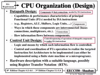
CPU Design
CPU Design. Introduction The CPU must perform three main tasks: Communication with memory Fetching Instructions Fetching and storing data Interpretation of Instructions Execution of Instructions. The CPU is endlessly looping through these steps


CPU Design
E N D
Presentation Transcript
Introduction • The CPU must perform three main tasks: • Communication with memory • Fetching Instructions • Fetching and storing data • Interpretation of Instructions • Execution of Instructions
The CPU is endlessly looping through these steps • Actual steps will vary from processor to processor • Typical steps 1. instruction fetch & Program Counter update 2. instruction decode & operand load 3. operation execution (control instructions update Program Counter) 4. memory access 5. register update
Generic CPU State Diagram • Fetch cycle: Fetch an instruction from memory, then go to the decode cycle. • Decode cycle: Decode the instruction – that is, determine which instruction has been fetched – then go to the execute cycle for that instruction. • Execute cycle; Execute the instruction, then go to the fetch cycle and fetch the next instruction.
Very Simple CPU – Additional Registers • Six bit address register, AR • Six bit program counter, PC • Eight bit data register, DR • Two bit instruction register, IR
Very Simple CPU – Fetching Instructions from Memory • Send the address to memory by placing it on the address pins A[5..0] • After allowing memory enough time to perform its internal decoding and to retrieve the desired instruction, send a signal to memory so that it outputs the instruction on its output pins. • The address is stored in the program counter, PC FETCH1: AR PC • CPU asserts a READ signal and increments PC FETCH2: DR M, PC PC + 1 • Copy two high order bits of DR to IR and six low-order bits of DR to AR FETCH3: IR DR[7..6], AR DR[5..0]
Fetch Cycle for Very Simple CPU FETCH1: AR PC FETCH2: DR M, PC PC + 1 FETCH3: IR DR[7..6], AR DR[5..0]
Fetch and Decode Cycles for Very Simple CPU ADD1: DR M ADD2: AC AC + DR JMP1: PC DR[5..0] AND1: DR M AND2: AC AC ^ DR INC1: AC AC + 1
Complete State Diagram for Very Simple CPU This diagram includes the data paths for all the operations
Establishing Required Data Paths • Operations associated with each state of the CPU are: FETCH1: AR PC FETCH2: DR M, PC PC + 1 FETCH3: IR DR[7..6], AR DR[5..0] ADD1: DR M ADD2: AC AC + DR AND1: DR M AND2: AC AC ^ DR JMP1: PC DR[5..0] INC1: AC AC + 1
Establishing Required Data Paths • Regroup the operations, without regard for the cycles in which they occur, by registers whose contents they modify. AR: AR PC; AR DR[5..0] PC: PC PC + 1; PC DR[5..0] DR: DR M IR: IR DR[7..6] AC: AC AC + DR; AC AC ^ DR; AC AC + 1 • Connect every component to the system bus
Preliminary Register Section for the Very Simple CPU Simple Observations: AR only supplies its data to memory – don’t need to connect to any other component IR does not supply data to any other component via the internal bus – can remove output connection AC does not supply its data to any component – remove connection to internal bus The bus is 8 bits wide, but not all data transfers are 8 bits (some are 6, some are 2) – need to specify which registers send and receive to and from which bus AC must be able to load the sum of AC and DR, logical AND of AC and DR. CPU needs to include an ALU to do that.