CPU Structure and Function
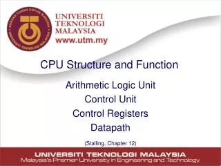
CPU Structure and Function. Arithmetic Logic Unit Control Unit Control Registers Datapath (Stalling, Chapter 12). Arithmetic Logic Unit (ALU) Complementor Adder Shifter Control logic Hardwired/Microprogram Temporary storage General purpose registers Specialized purpose registers.

CPU Structure and Function
E N D
Presentation Transcript
CPU Structure and Function Arithmetic Logic Unit Control Unit Control Registers Datapath (Stalling, Chapter 12)
Arithmetic Logic Unit (ALU) Complementor Adder Shifter Control logic Hardwired/Microprogram Temporary storage General purpose registers Specialized purpose registers CPU Component
CPU Overview • ALU • Actual computation or processing data • Control logic • Control movement of data and instructions into and out of CPU • Registers • General & Special Purpose • Storage location for intermediate data
Internal CPU bus to transfer data between registers and ALU Internal Structure of CPU
Register Organization • Registers form the highest level of the memory hierarchy. • Small set of high speed storage locations • Temporary storage for data and control information • Two types of registers: • User-visible (General purpose)May be referenced by assembly-level instructions and are thus “visible” to the user. • Control and status registers (Special purpose)Used to control the operation of the CPU.Most are not visible to the user.
User-Visible Registers • General purpose registers • Can be assigned to a variety of functions. • Defined to the operations within the instructions. • Can be used for addressing functions • Data registers • Hold data and cannot be used in the calculation of an operand address. • Example accumulator • Address registers • Hold address information. • Examples: general purpose address registers, segment pointers, stack pointers, index registers.
User-Visible Registers • Condition codes or Flags • Bits set by the processor hardware as a result of operations • Can be accessed by a program but not changed directly • Examples: • sign flag • zero flag • overflow flag • Bit values are used as the basis for conditional jump instructions.
Flags Affected by Arithmetic Operations • The ALU has a number of status flags that reflect the outcome of arithmetic (and bitwise) operations • based on the contents of the destination operand • Essential flags: • Zero flag : set when destination equals zero • Sign flag : set when destination is negative • Carry flag : set when unsigned value is out of range • Overflow flag : set when signed value is out of range • Auxillary flag : set when there is carry from lower nibble to higher nibble in the lower byte • Parity flag : set when there are odd or even number of 1’s in the lower byte
Example 1: Flags • Assuming that the system uses even parity • The following operation: 06 h 0 0 0 0 0 1 1 0 + 54 h 0 1 0 1 0 1 0 0 5A h => 0 1 0 1 1 0 1 0 Carry flag: 0 Sign flag: 0 Auxiliary carry flag: 0 Parity flag: 1 Zero flag: 0 Overflow flag: 0
Example 2: Flags (Odd Parity) 2FH + DEH 0010 1111 + 1101 1110 -------------------- 1 0000 1101 OF =0, CF = 1, PF = 1, AF = 1, ZF = 0, SF = 0 5432H + 7098H 0101 0100 0011 0011 + 0111 0000 1001 1000 -------------------------------- 1100 0100 1100 1011 OF =1, CF = 0, PF = 0, AF = 0, ZF = 0, SF = 1
Example 3: Flags (Odd parity) 3CH – 28H 0011 1100 + 1101 1000 Two’s complement for 28H ------------------ 1 0001 0100 OF =0, CF = 1, PF = 0, AF = 1, ZF = 0, SF = 0 5AH – 7FH 0101 1010 + 1000 0001 Two’s complement for 7FH ------------------- 1101 1011 OF =0, CF = 0, PF = 0, AF = 0, ZF = 0, SF = 1
Design Trade Off: General Purpose and Specialized Registers • General purpose registers maximize flexibility in instruction design. • Special purpose registers permit implicit register specification in instructions – reduces register field size in an instruction. • No clear “best” design approach.
How many registers are enough? • More registers permit more operands to be held within the CPU -- reducing memory bandwidth requirements to some extent. • More registers cause an increase in the field sizes needed to specify registers in an instruction word. • Most machines use 8-32 registers.
How big (wide) ? • Address registers should be wide enough to hold the longest address! • Data registers should be wide enough to hold most data types. • Would not want to use 64-bit registers if the vast majority of data operations used 16 and 32-bit operands. • Related to width of memory data bus. • Concatenate registers together to store longer formats.
Control and Status Registers • Registers that are used during fetching, decoding and execution of instructions • Many are not visible to the user/programmer • Some are visible but can not be (easily) modified
ALU • Consist of functional units • Arithmetic operations: +, -, *, / • Boolean operations: OR, AND, NOT, ExOR • Comparision operations: <, >, =… • Co-processor for mathematical operations, floating point operations • RISC (Reduced Instruction Set Computers) • Have more than one functional units • Functional units can also be implemented using pipeline architecture (pipeline concept will be discussed later).
ALU Input and Output Components ALU Control Unit PSW/EFLAGS/FLAGS Registers Registers
Instruction Execution • We have learnt that instructions are executed sequentially. • The process of theexecution of an instruction consists of several steps which is referred to as instruction cycle. • Each step in the instruction cycle consists of several sequence smaller steps known as micro-operation.
Instruction Cycle Flow of data and information between registers during the instruction cycle varies from processor to processor.
Stages in Instruction Cycle • Fetch the instruction • Decode it • Fetch operands, if required • Perform the operation • Store results, if required • Recognize pending interrupts Fetch Cycle Execute Cycle
Micro-Operations • Every step of the instruction cycle consist of micro-operation(s) that are executed at specified time. • Every micro-operations is activated and control based on the signals from the control unit. • Example of micro-operations: • Transferring data from one register to another • Activating the functional unit of ALU • Conventional format using register transfer language (RTL) • Example: IP/PC IP/PC +1
Instruction Cycle: Fetch Cycle • 4 registers are involved: IP/PC, MAR, MBR and IR • The fetch cycle can be written symbolically using RTL as t1: MAR IP/PC t2: MBR [MAR]; IP/PC IP/PC + 1 t3: IR MBR t1, t2, t3 is the timing sequence
Fetch Cycle • t1: Content of IP/PC that points to the next address of the instruction to be executed is loaded to MAR and transferred to memory on the address bus. Next, CU will activate the read signal of the memory. • t2: Instruction is accessed from the memory and transfer to CPU on the data bus. This instruction will be loaded into MBR. At the same time, IP/PC will be incremented so as to point to the next instruction to be executed. • t3: Instruction in MBR is loaded into IR. The opcode of the instruction will be decoded and translated so as to determine the micro-operations for the particular instruction.
Rules for Clock Cycle Grouping • Proper sequence must be followed • MAR <- (IP/PC) must precede MBR <- (memory) • Conflicts must be avoided • Must not read & write same register at same time • MBR <- (memory) & IR <- (MBR) must not be in same cycle • Also: IP/PC <- (IP/PC)+1 involves addition • Use ALU • May need additional micro-operations
Indirect Cycle • Involve with fetching data from memory before initiating the execute cycle. • Example: ADD AX, [2400] • In this cycle, the operand bits of the instruction that is in IR are transferred to MAR. The read control line is activated and the data associated with the address will be read and transfer to MBR. t1 : MAR IR [operand/address] t2 : MBR Mem[MAR] t3: IR[operand] MBR
Instruction Cycle: Execute Cycle • The opcode of the instruction in IR will be decoded and related control signals will be generated.
Example of Instruction Execution • ADD AX, BXCU will generate signal to ALU (adder) for the addition of the content of two registers, AX and BX and store the result in AX. • JMP NEXT (branch to the instruction at location NEXT ) CU will activate the path from MBR to MAR for the transfer of the address in the operand field (of the current instruction in IR) to fetch the next instruction.
Example 2: Opcode: 1 – LOAD 5 – ADD 2 - STORE
THE INSTRUCTIONS • The PC contains 300, the address of the first instruction. This instruction (the value 1940 in hexadecimal) is loaded into the instruction register IT and the PC is incremented. • The first 4 bits in the IR indicate that the AC is to be loaded. The remaining 12 bits specify the address (940) from which data are to be loaded. • The next instruction (5941) is fetched from location 301 and the PC is incremented. • The old contents of the AC and the contents of location 941 are added and the result is stored in the AC. • The next instruction (2941) is fetched from location 302 and the PC is incremented. • The contents of the AC are stored in location 941.
Example 3: MOV AX, NUM Fetch Cycle Address Data Control Bus Bus Bus MAR IP/PC Memory CU MBR IR AX
… Example 3 Clock IP/PC MAR MBR IR AX µoperation t0 100 - - - - IP/PC= 100 t1 100 100 - - - fetch cycle: MAR IP/PC; t2 101 100 4450 - - MBR [MAR]; IP/PC IP/PC +1; t3 101 100 4450 4450 - IR MBR indirect cycle: t4 101 450 4450 4450 - MAR IR[operand/address]; t5 101 450 000A 4450 - MBR Mem[MAR]; execution cycle: t6 101 450 000A 4450 000A AX MBR;
Control bus Address bus MAR IP/PC 0100 0100 0100 MOV AX, N 0101 0102 0103 N = FF CU MBR IR MOV AX, N Data bus 4 1 2 3 Example 4: MOV AX, N – Fetch Cycle
Control bus Address bus MAR IP/PC 2 0101 0103 0100 MOV AX, N 0101 0102 1 0103 N=FF CU N MBR FF IR MOV AX, N 3 Data bus Example 4: Indirect Cycle
Steps IP/PC MAR MBR IR AX Starting Value 0100 Fetch Cycle: MAR IP/PC 0100 MBR [MAR] Mov AX, N IP/PC IP/PC + 1 0101 IR MBR Mov AX, N Indirect Cycle: MAR IR[operand/address] [N]= 0103 MBR Mem[MAR] N=FF Execution Cycle AX MBR N=FF
Interrupt • The mechanism by which other system modules may interrupt the normal processing of the CPU. • These devices are 1-10 orders of magnitude slower than the CPU • CPU can waste vast amounts of processing cycles waiting for these slow devices to perform their tasks • Interrupts let the CPU execute its normal instruction sequence and pause to service the external devices only when they signal (the interrupts) that they are ready for the CPU’s attention. • The processor and the O/S are responsible for recognizing an interrupt, suspending the user program, servicing the interrupt, and then resuming the user program.
Cause for Interrupts • Mechanism by which other modules (e.g. I/O) may interrupt normal sequence of processing • Program • e.g. overflow, division by zero • Timer • Generated by internal processor timer • Used in pre-emptive multi-tasking • I/O • from I/O controller • Hardware failure • e.g. memory parity error
Interrupt Cycle • Interrupts are processed in an interrupt cycle within the overall instruction cycle. • At the end of an instruction cycle (operand storage step), check to see if any interrupts are pending. • If there aren’t any, proceed with the next instruction. • If there are, then: • Suspend execution of the program and save its “state”. • Jump to the interrupt service routine (ISR) and resume the “normal” instruction cycle. • When the ISR is completed, restore the state of the program and resume its operation.
Multiple Interrupts • Disable interrupts • Processor will ignore further interrupts whilst processing one interrupt • Interrupts remain pending and are checked after first interrupt has been processed • Interrupts handled in sequence as they occur • Define priorities • Low priority interrupts can be interrupted by higher priority interrupts • When higher priority interrupt has been processed, processor returns to previous interrupt