Download
1 / 26
260 likes | 458 Vues
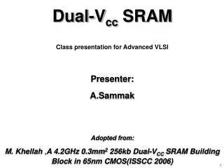
Dual-V cc SRAM Class presentation for Advanced VLSI Presenter: A.Sammak Adopted from: M. Khellah , A 4.2GHz 0.3mm 2 256kb Dual-V CC SRAM Building Block in 65nm CMOS(ISSCC 2006). Outline. Motivation Dual-V CC SRAM architecture Chip Implementation Measurement results Summary.

E N D
Dual-Vcc SRAM Class presentation for Advanced VLSI Presenter: A.Sammak Adopted from: M. Khellah ,A 4.2GHz 0.3mm2 256kb Dual-VCC SRAM Building Block in 65nm CMOS(ISSCC 2006)
Outline • Motivation • Dual-VCC SRAM architecture • Chip Implementation • Measurement results • Summary
Motivation • Increase bit density in LLC • Achieve the best energy efficiency
Voltage Effect on Density • Aggressive VMIN reduces bit density
Dual-VCC SRAM Architecture 1 . 2 V µP Core V = CORE 0 . 7 V 0 . 6 V ( standby ) . . . . V = 1 . 2 V LLC LLC • Dynamic VCORE and frequency scaling • VLLC≈ VMAX enables smallest cell in LLC L0 to L2 cashes
Dual-VCC 256Kb Block • Cut energy with stability considered • Shifters for Timer, WL & Write drivers
Explicit Level Shifter Signals from mid-logic to timer: clock, RD/WR enables and sub-array selects
Single & Dual-VCC Word-Line Driver Static NAND gate changed to dynamic
Single & Dual-VCC Write Driver Static CMOS changed to Dyn-CVSL
Level Shifter Comparison Scheme 1 Scheme 2 This work few shifters shifters for WL & Write drivers embedded shifters for WL & Write drivers
Level Shifter Comparison Embedded shifters reduce power & area this work
Passive Virtual Ground Clamp programmable passive clamp sleep • Wide Vss range due to PVT & aging
Active Virtual Ground Clamp programmable active clamp • Set VREF based on standby VMIN only • Continuously tracks PVT & aging
Active Power Management Deactivate based on leakage
Chip Micrograph Single-VCC 256Kb block with no sleep 2 Dual-VCC 256Kb blocks with sleep transistor
Measured Frequency and Power VLLC = 1.2V T = 85oC 5% Activity Standby VMIN = 0.9V • Dual-VCC block runs at 2.3-4.2GHz • 16-30mW for VCORE = 0.7-1.2V
Measured Leakage Power T = 85oC T = 25oC no retention • Leakage reduced by 30-60% for increase 2% area • 75% reduction for disabled blocks
Measured Power Vs. Activity 70 VLLC = 1.2V T = 85oC VMIN = 0.9V Without Sleep 60 ٌWith Sleep 50 40 Total Power (mW) 30 20 +5% at 33% 10 0 0.001 0.01 1 0.1 -10% at 5% -23% at 1% Activity Power including dynamic overhead reduced by 23% at 1% activity
Measured Tolerance to Process VLLC = 1.2V T = 85oC 10 dies Active clamp is within few mV of VMIN
Tolerance to Temperature 0.98 active (V) 0.96 passive SS -VV 0.94 LLC V 0.92 0.90 0 20 40 60 80 100 o T ( C) -14% • Passive clamp bias set for highest T • Active clamp saves 14-24% in leakage
Measured Tolerance to Voltage -24% • Passive clamp bias set for lowest VLLC • Active clamp saves 24% in leakage
Measured Tolerance to Aging VLLC = 1.2V VREF = 0.3V Aging: Read/Write/24 hours/100MHz/1.6V/110oC Active clamp is not affected by aging
Dual-VCCµP Power Reduction Power Voltage Core 64Mb Total Area Single-V µP 1.0V 1.00 1.00 1.00 1.000 CC Dual-V µP CC 0.24 1.00 0.74 1.002 V = 0.7V CORE with no sleep Dual-V µP V = 1.0V CC 0.24 0.85 0.65 1.032 LLC with sleep • 35% reduction in total µP power • Area: 3.2% cache area overhead
Summary • Dual-VCC 256Kb SRAM block in 65nm process • Consumes 16-30mW at 2.3-4.2 GHz using VCORE = 0.7V-1.2V & VLLC = 1.2V • Embedded shifters and active clamp • 35% reduction in µP total power