DIGITAL CARRIER MODULATION SCHEMES
DIGITAL CARRIER MODULATION SCHEMES. Dr.Uri Mahlab. 1. Dr. Uri Mahlab. INTRODUCTION. In order to transmit digital information over * bandpass channels, we have to transfer the information to a carrier wave of .appropriate frequency We will study some of the most commonly *


DIGITAL CARRIER MODULATION SCHEMES
E N D
Presentation Transcript
DIGITAL CARRIER MODULATION SCHEMES Dr.Uri Mahlab 1
Dr. Uri Mahlab INTRODUCTION In order to transmit digital information over * bandpass channels, we have to transfer the information to a carrier wave of .appropriate frequency We will study some of the most commonly * used digital modulation techniques wherein the digital information modifies the amplitude the phase, or the frequency of the carrier in .discrete steps 2
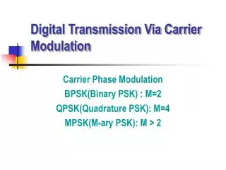
Dr. Uri Mahlab The modulation waveforms fortransmitting :binary information over bandpass channels ASK FSK PSK DSB 3
Dr. Uri Mahlab OPTIMUM RECEIVER FOR BINARY :DIGITAL MODULATION SCHEMS The function of a receiver in a binary communication * system is to distinguish between two transmitted signals .S1(t) and S2(t) in the presence of noise The performance of the receiver is usually measured * in terms of the probability of error and the receiver is said to be optimum if it yields the minimum .probability of error In this section, we will derive the structure of an optimum * receiver that can be used for demodulating binary .ASK,PSK,and FSK signals 4
Dr. Uri Mahlab Description of binary ASK,PSK, and : FSK schemes -Bandpass binary data transmission system Transmit carrier Local carrier Noise (n(t Clock pulses + Input ּ+ Binary data + (V(t (Z(t {bk} {bk} 5
:Explanation *The input of the system is a binary bit sequence {bk} with a * .bit rate r b and bit duration Tb The output of the modulator during the Kth bit interval * .depends on the Kth input bit bk The modulator output Z(t) during the Kth bit interval is * a shifted version of one of two basic waveforms S1(t) or S2(t) and :Z(t) is a random process defined by Dr. Uri Mahlab .1 6
Dr. Uri Mahlab The waveforms S1(t) and S2(t) have a duration * of Tb and have finite energy,that is,S1(t) and S2(t) =0 if and Energy :Term 7
Dr. Uri Mahlab :The received signal + noise 8
Choice of signaling waveforms for various types of digital* modulation schemes S1(t),S2(t)=0 for .The frequency of the carrier fc is assumed to be a multiple of rb Type of modulation ASK PSK FSK 0 9 Dr. Uri Mahlab
Dr. Uri Mahlab :Receiver structure (V0(t output Sample every Tb seconds 10
Dr. Uri Mahlab :{Probability of Error-{Pe* The measure of performance used for comparing * !!!digital modulation schemes is the probability of error The receiver makes errors in the decoding process * !!! due to the noise present at its input The receiver parameters as H(f) and threshold setting are * !!!chosen to minimize the probability of error 11
Dr. Uri Mahlab :The output of the filter at t=kTb can be written as * 12
:The signal component in the output at t=kTb h( ) is the impulse response of the receiver filter* ISI=0* 13 Dr. Uri Mahlab
Dr. Uri Mahlab Substituting Z(t) from equation 1 and making* change of the variable, the signal component :will look like that 14
:The noise component n0(kTb) is given by * .The output noise n0(t) is a stationary zero mean Gaussian random process :The variance of n0(t) is* :The probability density function of n0(t) is* 15 Dr. Uri Mahlab
Dr. Uri Mahlab The probability that the kth bit is incorrectly decoded* :is given by .2 16
Dr. Uri Mahlab :The conditional pdf of V0 given bk = 0 is given by* .3 :It is similarly when bk is 1* 17
Dr. Uri Mahlab Combining equation 2 and 3 , we obtain an* :expression for the probability of error- Pe as .4 18
:Conditional pdf of V0 given bk :The optimum value of the threshold T0* is* 19 Dr. Uri Mahlab
Dr. Uri Mahlab Substituting the value of T*0 for T0 in equation 4* we can rewrite the expression for the probability :of error as 20
Dr. Uri Mahlab The optimum filter is the filter that maximizes* the ratio or the square of the ratio (maximizing eliminates the requirement S01<S02) 21
Dr. Uri Mahlab :Transfer Function of the Optimum Filter* The probability of error is minimized by an * appropriate choice of h(t) which maximizes Where And 22
Dr. Uri Mahlab If we let P(t) =S2(t)-S1(t), then the numerator of the* :quantity to be maximized is Since P(t)=0 for t<0 and h( )=0 for <0* :the Fourier transform of P0 is 23
:Hence can be written as* (*) We can maximize by applying Schwarz’s* :inequality which has the form (**) 24 Dr. Uri Mahlab
Applying Schwarz’s inequality to Equation(**) with- and We see that H(f), which maximizes ,is given by- (***) !!! Where K is an arbitrary constant 25 Dr. Uri Mahlab
Dr. Uri Mahlab Substituting equation (***) in(*) , we obtain- :the maximum value of as :And the minimum probability of error is given by- 26
Dr. Uri Mahlab :Matched Filter Receiver* If the channel noise is white, that is, Gn(f)= /2 ,then the transfer - :function of the optimum receiver is given by From Equation (***) with the arbitrary constant K set equal to /2- :The impulse response of the optimum filter is 27
Dr. Uri Mahlab Recognizing the fact that the inverse Fourier * of P*(f) is P(-t) and that exp(-2 jfTb) represent :a delay of Tb we obtain h(t) as :Since p(t)=S1(t)-S2(t) , we have* The impulse response h(t) is matched to the signal * :S1(t) and S2(t) and for this reason the filter is called MATCHED FILTER 28
:Impulse response of the Matched Filter * (S2(t 1 t 0 2 \Tb (a) (S1(t 0 2 \Tb t 1- (b) 2 (P(t)=S2(t)-S1(t 2 \Tb 0 t Tb 2 (c) (P(-t t (d) Tb- 0 2 (h(Tb-t)=p(t (h(t)=p(Tb-t 2 \Tb 0 t 29 (e) Tb Dr. Uri Mahlab
Dr. Uri Mahlab :Correlation Receiver* The output of the receiver at t=Tb* Where V( ) is the noisy input to the receiver Substituting and noting * : that we can rewrite the preceding expression as (# #) 30
Dr. Uri Mahlab Equation(# #) suggested that the optimum receiver can be implemented * as shown in Figure 1 .This form of the receiver is called A Correlation Receiver integrator Figure 1 Threshold device (A\D) - + Sample every Tb seconds integrator 31
In actual practice, the receiver shown in Figure 1 is actually * .implemented as shown in Figure 2 In this implementation, the integrator has to be reset at the - (end of each signaling interval in order to ovoid (I.S.I !!! Inter symbol interference :Integrate and dump correlation receiver White Gaussian noise Closed every Tb seconds (n(t Filter to limit noise power Threshold device (A/D) + + c R (Signal z(t High gain amplifier Figure 2 The bandwidth of the filter preceding the integrator is assumed * !!! to be wide enough to pass z(t) without distortion 32 Dr. Uri Mahlab
Dr. Uri Mahlab Example: A band pass data transmission scheme uses a PSK signaling scheme with The carrier amplitude at the receiver input is 1 mvolt and the psd of the A.W.G.N at input is watt/Hz. Assume that an ideal correlation receiver is used. Calculate the .average bit error rate of the receiver 33
:Solution Dr. Uri Mahlab Data rate =5000 bit/sec Receiver impulse response Threshold setting is 0 and 34
:Solution Continue Dr. Uri Mahlab =Probability of error = Pe * From the table of Gaussian probabilities ,we* get Pe 0.0008 and Average error rate (rb) pe /sec = 4 bits/sec 35