New Build Up Process
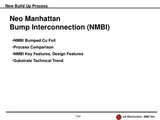
New Build Up Process. Neo Manhattan Bump Interconnection (NMBI). NMBI Bumped Cu Foil Process Comparison NMBI Key Features, Design Features Substrate Technical Trend. 7/24. LG Electronics / DMC Div. NMBI. NMBI - Etched Cu Bump with Cu Foil. NMBI. Cu Foil. NMBI Cu Bump(SEM). Cu Bump.

New Build Up Process
E N D
Presentation Transcript
New Build Up Process Neo Manhattan Bump Interconnection (NMBI) • NMBI Bumped Cu Foil • Process Comparison • NMBI Key Features, Design Features • Substrate Technical Trend 7/24 LG Electronics / DMC Div.
NMBI NMBI - Etched Cu Bump with Cu Foil NMBI Cu Foil NMBI Cu Bump(SEM) Cu Bump NMBI + B2it NMBI Mass Lam (2+2+2) 8/24 LG Electronics / DMC Div.
NMBI New Development of Core PCB Interconnect Method A very stable electrical & Mechanical interconnect structure has been achieved Cu/Cu Metallic Connection Zoom in • High Reliability compared to • convention Cu plated TH, • Fine Interconnection for • High Density PCB 9/24 LG Electronics / DMC Div.
NMBI Production Process Comparison Process Photo-via,Laser-via B2it(Toshiba) NMBI + B2it Cross section Diagram • Min via Dia. • Min Land Dia. • Stacked Via Φ 200 ㎛ Φ 300 ㎛ Possible Φ 150 ㎛ Φ 300 ㎛ Impossible Less than Φ 100 ㎛ Less than Φ 200 ㎛ Possible • Simplified process enables cost reduction • Enables easier stacking of via Strong points • Enable easier reduction • of via sizes • One-step batch processing • of various via sizes Weak points Difficult to reduce via diameter Not possible to form via of difference size in a one-step process Numerous process steps Significant time required for via formation Significant capital investment required for laser equipment Thermal excursions and surface planarization induce dimensional instability, making multi-layer build -up structures more difficult to fabricate 10/24 LG Electronics / DMC Div.
NMBI 12/24 LG Electronics / DMC Div.
NMBI 13/24 LG Electronics / DMC Div.
NMBI High Density Design • Land-less • Fine Pitch Pattern • Fine Pitch Bump(Via) NMBI - Land-less Laser Via Number of Lines 14/24 LG Electronics / DMC Div.
NMBI(Key Feature) 15/24 LG Electronics / DMC Div.
NMBI(Key Feature) 16/24 LG Electronics / DMC Div.
NMBI NMBI(Key Feature) 17/24 LG Electronics / DMC Div.
NMBI NMBI(Key Feature) 18/24 LG Electronics / DMC Div.
NMBI 19/24 LG Electronics / DMC Div.
Reliability Test Results Spec. No Item Condition Result 1 Peel Strength Peeling Speed 500mm/min 1.0kg/cm OK OK 2 Insulating Voltage DC500V, 60sec No damage OK 3 Pads Pull Strength 90/ Pull head Speed :10mm/min 2kg/mm2 4 260℃(10sec)⇔20℃(20sec) 100Cycle Conductivity Changing Ratio less than 10% OK Hot Oil (Thermal Shock) Conductivity Changing Ratio less than 10% 5 OK Bending ±10% Bending 100 Cycle OK 6 2mOhm/Via Via Resistance 20/24 LG Electronics / DMC Div.