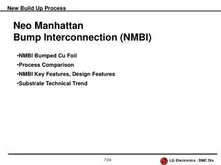
New build-up technique with copper bump
New build-up technique with copper bump. AGP Process. AGP Build-up PCB. AGP Build-up PCB Section Figure. Multi-via Structures. Cross sectional view of AGP. To use copper bump as a connection between layers. Photo. 1+4+1 build-up PWB using AGP. Cross sectional view of AGP. Copper bump.

New build-up technique with copper bump
E N D
Presentation Transcript
New build-up techniquewith copper bump AGP Process
AGP Build-upPCB Section Figure Multi-via Structures
Cross sectional view of AGP To use copper bump as a connection between layers Photo. 1+4+1 build-up PWB using AGP
Cross sectional view of AGP Copper bump L1 alnd L2 land Photo. 2+2+2 build-up PWB using AGP Photo. 3+4+3 build-up PWB using AGP
Concepts of developing AGP 1.Possible to reduce land size 2.Possible to stack vias 3. Possible to form bumps of different diameters in a one-step batch process 4. Improvement of reliability of electrical connection
Benefits of AGP • 1. Possible to reduce diameter of via • AGP bump is formed by etching • method. • It is possible to form micro-bumps • with a diameter 50micron. 2. Possible to stack vias easily AGP enables very flat land surface without via-filling. It is suitable process for multi-layer build-up structure.
Benefits of AGP 3. High reliability of connecting Land to via joining is achieved by copper plating. This enables high reliability of electrical connection and high land- pull strength. 4. Possible to form bumps of different diameters By selecting the size of the etching mask, the bump of a different diameter can exist together. Larger bump can be used for the part where high heat conductivity or low electric resistance are necessary.
Benefits of AGP 5. Low surface roughness of outer copper Outer layer is formed by panel-plating. It has sufficient peel strength even if there is no anchor effect. This smooth side contributes to the high frequency characteristic.
Structure that AGP enables 1. Multi build-up structure with stacking via High density PWBs can be achieved by AGP. 2. Flip chip pad with micro via connection It is suitable for MCM.
Structure that AGP enables Via and line can be connected directly without forming land. It will bring drastic higher wiring density. 3. Land-less pattern 3D view Upper view 4. Rigidly improvement by copper frame Because the bump layer is formed by the etching, It is possible to process it to various shape. That enables frame as illustrated, it brings rigidly Improvement. It is also as possible to build the coaxial cable Structure into.
Structure that AGP enables 5. Heat management by forming thermal via BGA/CSP Forming chip size heat sink By AGP process Plugged via by using Conductive paste Improvement of heat dissipation effect
Schematic illustration of AGP process Core board Copper plated on core board Forming bumps by etching Forming dielectric layer(Liquid epoxy) Copper plating as outer layer
Inner Layer Pattern AGP Process
Copper Plating AGP Process
Bump Masking AGP Process
Bump Etching AGP Process
Dielectric layer AGP Process
External Layer Pattern AGP Process
Manufacturing Spec Minimum land size of outer layer 100m Minimum size of top of via 50m Dielectric thickness of AGP layer 30~60m Dielectric consists of epoxy resin Not including glass-cross Minimum size of bottom of via 75m Minimum land size of inner layer 150 m