Download
1 / 5
50 likes | 173 Vues
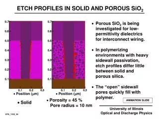
ETCH PROFILES IN SOLID AND POROUS SiO 2. Porous SiO 2 is being investigated for low-permittivity dielectrics for interconnect wiring. In polymerizing environments with heavy sidewall passivation, etch profiles differ little between solid and porous silica.

E N D
ETCH PROFILES IN SOLID AND POROUS SiO2 • Porous SiO2 is being investigated for low-permittivity dielectrics for interconnect wiring. • In polymerizing environments with heavy sidewall passivation, etch profiles differ little between solid and porous silica. • The “open” sidewall pores quickly fill with polymer. Position (m) Position (m) Porosity = 45 % Pore radius = 10 nm ANIMATION SLIDE Solid University of Illinois Optical and Discharge Physics UTA_1102_36
EFFECT OF PORE RADIUS ON CLEANING • Larger pores have poor view angles to ions and thicker polymer layers. • Lower rate of cleaning results. 4 nm 16 nm • Ar/O2=99/1, 40 sccm, 600 W, 4 mTorr University of Illinois Optical and Discharge Physics ANIMATION SLIDE GEM_0204_28
CLEANING INTERCONNECTED PORES • Cleaning is inefficient with interconnected pores. • Higher interconnectivity leads to larger shadowing of ions. 100% 0% 60% • Interconnectivity • Ar/O2=99/1, 40 sccm, 600 W, 4 mTorr University of Illinois Optical and Discharge Physics ANIMATION SLIDE GEM_0204_29
MIN MAX POLYMER SURFACE STRUCTURES Animation Slide The avalanche exposes the tubules to a burst of hot electrons, unevenly charging surfaces. Ion fluxes are also uneven. Electron density Electron Temperature • N2/O2/H2O =79.5 / 19.5 / 1, 1 atm, 15 kV, 2.5 ns University of Illinois Optical and Discharge Physics GEM_0204_41
MIN MAX RESOLVING POLYMER SURFACE STRUCTURES The avalanche exposes the tubules to a burst of hot electrons, unevenly charging surfaces. Ion fluxes are also uneven. M+ density Charge density Animation Slide • N2/O2/H2O =79.5 / 19.5 / 1, 1 atm, 15 kV, 2.5 ns University of Illinois Optical and Discharge Physics GEM_0204_42