Combinational Circuit Design
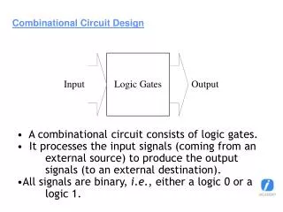
Combinational Circuit Design. A combinational circuit consists of logic gates. It processes the input signals (coming from an external source) to produce the output signals (to an external destination). All signals are binary, i . e ., either a logic 0 or a logic 1.

Combinational Circuit Design
E N D
Presentation Transcript
Combinational Circuit Design • A combinational circuit consists of logic gates. • It processes the input signals (coming from an external source) to produce the output signals (to an external destination). • All signals are binary, i.e., either a logic 0 or a logic 1.
Combinational Circuit Design • All signals may have 1 or 2 lines. • If 1 line, represents either the normal (unprimed) variable or the complement (primed). • If 2 lines, both primed and unprimed variables are represented. It is assumed that one is always the complement of the other. • Unless stated, it shall be assumed that 2 lines are available for each of the input signals.
Design Procedure 1. Problem Statement • The specification is normally in plain language explaining how the circuit is supposed to function. • The designer needs to rely on intuition and experience to arrive at the correct interpretation of the problem.
Design Procedure 2. Problem Analysis • Identify the inputs and the outputs. • Assign variables to the inputs and outputs. • Determine the relationship between the inputs and the outputs. This can either be in the form of a truth table showing the relationship, or a simple Boolean expression derivable from the problem.
Design Procedure • Logic Circuit Design • Simplify the Boolean expression. • Boolean Algebra • Karnaugh Map • Draw the corresponding logic diagram.
Combinational Circuit Design Problem 1 Problem The Last Rogue's Bank wants to set up a simple security system. This is to be connected directly to an alarm at the Police Station for immediate response. There shall be a switch (T) at the teller's window to trigger the alarm when a robbery is in progress. After the bank closes, a main switch (M) shall be turned on to enable the sensors within the bank. One sensor shall be placed on the only door into the bank (D). This shall trigger the alarm when the door is opened if the main switch is on unless a secret outside switch (S) is turned on by a special key.
Combinational Circuit Design Problem 1 Another sensor shall be placed on the vault door (V). This shall trigger the alarm when the vault is opened if the main switch is on. The bank president shall have a switch by his desk (P) which when turned on by his key will disable the security system. This is in case the president wants to rob the bank himself. Design a combinational logic circuit which will generate the signal (A) that will turn on the police station alarm as specified above.
Combinational Circuit Design Problem 1 Solution Solution • Input signals T Teller's switchM Main switchD Front door sensorS Secret outside switchV Vault door sensorP President's switch
Combinational Circuit Design Problem 1 Solution • Output signal A Police station alarm • When does the alarm go off? • If one of the following conditions is satisfied: • Teller turns on switch (T). • Front door opens when main switch is on and secret outside switch is off ( ). • Vault door is opened when main switch is on and president's switch if off (VM). • Unless the president's switch if turned on.
Combinational Circuit Design Problem 1 Solution • Output function • Circuit Diagram

