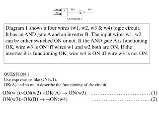
Download
1 / 40
400 likes | 599 Vues
Presentation 12 MAD MAC 525. Farhan Mohamed Ali (W2-1) Jigar Vora (W2-2) Sonali Kapoor (W2-3) Avni Jhunjhunwala (W2-4). W2. Design Manager: Zack Menegakis. 26 th April, 2006 Short Final Presentation. Project Objective:

E N D
Presentation 12 MAD MAC 525 Farhan Mohamed Ali (W2-1)Jigar Vora (W2-2)Sonali Kapoor (W2-3)Avni Jhunjhunwala (W2-4) W2 Design Manager: Zack Menegakis 26th April, 2006 Short Final Presentation Project Objective: Design a crucial part of a GPU called the Multiply Accumulate Unit (MAC) which will revolutionize graphics.
Agenda • Marketing (Jigar) • Project Description (Farhan) • Algorithmic Description (Farhan) • Design Process (Sonali) • Floorplan Evolution (Sonali) • Layout (Avni) • Design Specifications (Avni) • Conclusion (Jigar)
MARKETING • Application of product: HDR rendering in gaming graphics • Why HDR? Used in games like Far Cry • Optimization for speed( chose this because of market) • Competition- if enter market, possible barriers to entry
MAD MAC and HDR • What is HDR? • Show animation explaining concept
MAD MAC and HDR • MAD MAC accelerates FP16 blending to enable true HDR graphics • What is HDR? • HDR = High Dynamic Range • Dynamic range is defined as the ratio of the largest value of a signal to the lowest measurable value • Dynamic range of luminance in real-world scenes can be 100,000 : 1 • With HDR rendering, pixel intensity are allowed to extend beyond [0..1] range of traditional graphics • Nature isn’t clamped to [0..1] and neither should CG • In lay terms: • Bright things can be really bright • Dark things can be really dark • And the details can be seen in both
PROJECT DESCRIPTION • Multiply Accumulate unit (MAC) • Executes function AB+C on 16 bit floating point inputs. Inputs will be OpenEXR format. • Multiply and add in parallel to greatly speed up operation • Rounding is only performed only once so greater accuracy than individual multiply and add functions. • Also known as: • Fused Multiply Add (FMA) • Multiply Add (MAD/MADD) in graphics shader programs • Many applications benefit from a fast FMA • Graphics – HDR rendering, blending and shader ops • DSPs – computing vector dot-products in digital filters • Fast division, square root – eliminates extra hardware • Available in many newer CPUs and DSPs because it’s so cool • One ring (circuit) to rule them all!
ALGORITHMIC DESCRIPTION • Step through entire process • Multiply and align occurs concurrently- always align C to A*B • Outputs go to adder, normalize, round, overflow checker and output register
Block Diagram Input Input 16 Input 16 16 5 RegArray A RegArray B RegArray C 10 10 5 10 5 Multiplier Exp Calc Align 1 5 22 14 35 Control Logic & Sign Dtrmin Leading 0 Anticipator Adder/Subtractor 36 4 Normalize 14 1 5 Round Reg Y 1 10 5 15 16 Output 1 Ovf Checker
IMPLEMENTATION • Implementation of each module- how and why we chose a particular method keeping in mind goal of speed( multiplier, adder)
Design Decisions (contd.): • Multiplier Implementation • 11 x 11 Carry-Save Multiplier • Reasons: • Fast because it avoids having ripple carry in every stage • Enables Compact Layout
Design Process • Verilog-> Schematic-> Layout • Behavioral -> Structural Verilog • Transistors/gates -> Full Schematic • Gate/Component Layout -> Top Level • Transistor Count fluctuated from 20,200 to 12,800 • Major design decisions • Decided against implementing denormal arithmetic because it would increase the complexity of the project beyond the scope of the class • Round performed only once at the end. • Picked nPass over Tgate in the normalize shifter • Adder: variable length carry select-> Han-Carlson binary tree adder
VERIFICATION OF DESIGN Verilog Simulations ( show outputs) • Overview • How/Why it works • Behavioral/Structural Explain why we couldn’t get a high-level simulator and how we tested our verilog design.
SCHEMATICS • Show schematics of major blocks: adder, multiplier, and top-level • HOW WE VERIFIED: analog simulation
FLOORPLAN EVOLUTION • Initial floorplan • How it evolved (with animation)- why and how we changed it
Main Floorplan Multiplier Reg A Reg C Exp Calc Reg B Align C Pipeline Reg Pipeline Reg Adder Ld Zero Pipeline Reg Round Normalize Reg Y
Full Chip Layout Exponent Multiplier Zero Align Adder O v f N o r m a l i z e R o u n d
Pipelining • Initially planned 5-6 pipeline stages • Reduced to 4 pipeline stages – made possible by implementing fast carry lookahead adders in critical path modules (adder and multiplier)
Pipelining Stages Reg C Multiplier Reg A Exp Calc Reg B Pipeline Reg Pipeline Reg Align C Pipeline Reg Pipeline Reg Adder Ld Zero Pipeline Reg Round Normalize Overflow checker Reg Y
LAYOUT • Final Layout • Layout of large blocks such as multiplier, adder and normalize
Layout Decisions • 3 standard cell heights • Uniform width vdd and ground rails • Wider vdd and ground rails in power hungry modules • Max of 8 flip flops per clock pulse generator • Metal directionality
Design Specifications • Worst case delay = 2.25ns • Long buses are all buffered (not tested yet) • Estimated clocking speed = 400MHz • Height by width = 193.86 um * 301.545 um • Area = 58,458 um^2 • Aspect ratio = 1:1.55 • Total Transistor density = 0.22
Layout densities • Active : 14.05% • Poly : 9.25% • Metal 1 : 33.89% • Metal 2 : 18.00% • Metal 3 : 14.99% • Metal 4 : 6.29%
Conclusion • More marketing • Summarize chip functionality • Extending applications of chip