Overview of Computer Organization and Memory Systems for Final Exam Preparation
This lecture reviews essential concepts in computer organization, focusing on the central processing unit (CPU), memory systems, and instruction execution. Key topics include data paths, control signals, registers, instruction sequencing, and how different instruction types interact with the memory hierarchy. Students are reminded of the final exam schedule and review session details, emphasizing the importance of completing lab work and seeking extra credit opportunities.

Overview of Computer Organization and Memory Systems for Final Exam Preparation
E N D
Presentation Transcript
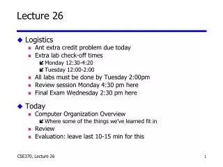
Lecture 26 • Logistics • Ant extra credit problem due today • Extra lab check-off times • Monday 12:30-4:20 • Tuesday 12:00-2:00 • All labs must be done by Tuesday 2:00pm • Review session Monday 4:30 pm here • Final Exam Wednesday 2:30 pm here • Today • Computer Organization Overview • Where some of the things we’ve learned fit in • Review • Evaluation: leave last 10-15 min for this
address Memory System Processor read/write data central processing unit (CPU) control signals Control Data Path data conditions instruction unit– instruction fetch and interpretation FSM execution unit– functional units and registers Structure of a computer • Block diagram view
OE Q7 Q6 Q5 Q4 Q3 Q2 Q1 Q0 LD D7 D6 D5 D4 D3 D2 D1 D0 CLK Registers • Selectively loaded – EN or LD input • Output enable – OE input • Multiple registers – group 4 or 8 in parallel OE asserted causes FF state to be connected to output pins; otherwise they are left unconnected (high impedance) LD asserted during a lo-to-hi clock transition loads new data into FFs
Instruction sequencing • Example – an instruction to add the contents of two registers (Rx and Ry) and place result in a third register (Rz) • Step 1: get the ADD instruction from memory into an instruction register (IR) • Step 2: decode instruction • instruction in IR has the code of an ADD instruction • register indices used to generate output enables for registers Rx and Ry • register index used to generate load signal for register Rz • Step 3: execute instruction • enable Rx and Ry output and direct to ALU • setup ALU to perform ADD operation • direct result to Rz so that it can be loaded into register
Instruction types • Data manipulation • add, subtract • increment, decrement • multiply • shift, rotate • immediate operands • Data staging • load/store data to/from memory • register-to-register move • Control • conditional/unconditional branches in program flow • subroutine call and return
Elements of the control unit (aka instruction unit) • Standard FSM elements • state register • next-state logic • output logic (datapath/control signalling) • Moore or synchronous Mealy machine to avoid loops unbroken by FF • Plus additional "control" registers • instruction register (IR) • program counter (PC) • Inputs/outputs • outputs control elements of data path • inputs from data path used to alter flow of program (test if zero)
Instruction execution • Control state diagram (for each diagram) • reset • fetch instruction • decode • execute • Instructions partitioned into three classes • branch • load/store • register-to-register • Different sequence throughdiagram for eachinstruction type Reset Init InitializeMachine FetchInstr. Load/Store ExecuteInstr. Branch Register-to-Register Branch Taken BranchNot Taken Incr.PC
Cin Ain FA Sum Bin Cout Ain Sum HA Bin Cout HA Cin Data path (hierarchy) • Arithmetic circuits constructed in hierarchical and iterative fashion • each bit in datapath is functionally identical • 4-bit, 8-bit, 16-bit, 32-bit , 64-bit datapaths
A B 16 16 Operation 16 N S Z Data path (ALU) • ALU block diagram • input: data and operation to perform • output: result of operation and status information
16 REG AC 16 16 OP N 16 Z Data path (ALU + registers) • Accumulator • special register • one of the inputs to ALU • output of ALU stored back in accumulator • One-address instructions • operation and address of one operand • other operand and destinationis accumulator register • AC AC op Mem[addr] • "single address instructions”(AC implicit operand) • Multiple registers • part of instruction usedto choose register operands
CO CO ALU CI ALU ALU CI AC AC AC rt R0 rs rt rd rd rs rt rd R0 rs R0 frommemory frommemory frommemory Data path (bit-slice) • Bit-slice concept – iterate to build n-bit wide datapaths 2 bits wide 1 bit wide
Instruction path • Program counter • keeps track of program execution • address of next instruction to read from memory • may have auto-increment feature or use ALU • Instruction register • current instruction • includes ALU operation and address of operand • also holds target of jump instruction • immediate operands • Relationship to data path • PC may be incremented through ALU • contents of IR may also be required as input to ALU
Data path (memory interface) • Memory • separate data and instruction memory (Harvard architecture) • two address busses, two data busses • single combined memory (Princeton architecture) • single address bus, single data bus • Separate memory • ALU output goes to data memory input • register input from data memory output • data memory address from instruction register • instruction register from instruction memory output • instruction memory address from program counter • Single memory • address from PC or IR • memory output to instruction and data registers • memory input from ALU output
Block diagram of processor • Register transfer view of Princeton architecture • which register outputs are connected to which register inputs • arrows represent data-flow, other are control signals from control FSM • MAR may be a simple multiplexer rather than separate register • MBR is split in two (REG and IR) • load control for each register load path 16 REG AC rd wr storepath 16 16 data Data Memory (16-bit words) OP addr N 8 Z ControlFSM MAR 16 IR PC 16 16 OP 16
load path 16 REG AC rd wr storepath 16 16 data Data Memory (16-bit words) OP addr N 16 Z ControlFSM 16 IR PC data Inst Memory (8-bit words) 16 16 OP addr 16 Block diagram of processor • Register transfer view of Harvard architecture • which register outputs are connected to which register inputs • arrows represent data-flow, other are control signals from control FSM • two MARs (PC and IR) • two MBRs (REG and IR) • load control for each register
“Why” take CSE 370 Required (okay, but let’s talk about why it is required and will be useful for your future) Most basic building blocks of computer science (0’s and 1’s) It is important to understand how they are used as baseline for more complex operations (adding, storing, other logic like if/while) It is good to understand what can be implemented in hardware, and why it is sometimes good to implement certain things in hardware instead of software Understand how some of the technology you interact with on daily basis (memory stick, vending machine, etc) at the hardware logic level. Knowledge gained in this course is used directly in industry/research
What you should know • Combinational logic basics • Binary/hex/decimal numbers • Ones and twos complement arithmetic • Truth tables • Boolean algebra • Basic logic gates • Schematic diagrams • Timing diagrams • de Morgan's theorem • AND/OR to NAND/NOR logic conversion • K-maps (up to 4 variables), logic minimization, don't cares • SOP, POS • Minterm and maxterm expansions (canonical, minimized) I like Pink and Blue but not Yellow…
What you should know • Combinational logic applications • Combinational design • Input/output encoding • Truth table • K-map • Boolean equation • Schematics • Multiplexers/demultiplexers • PLAs/PALs • ROMs • Adders 4529 + 34532 ------------- ????
What you should know • Sequential logic building blocks • Latches (R-S and D) • Flip-flops (D and T) • Latch and flip-flop timing (setup/hold time, prop delay) • Timing diagrams • Asynchronous inputs and metastability • Registers Remember that the last number was 1
What you should know • Counters • Timing diagrams • Shift registers • Ring counters • State diagrams and state-transition tables • Counter design procedure 1. Draw a state diagram 2. Draw a state-transition table 3. Encode the next-state functions 4. Implement the design • Self-starting counters 1, 2, 3, 4, …
What you should know (Final exam focus is here though exam is cumulative) • Finite state machines • Timing diagrams (synchronous FSMs) • Moore versus Mealy versus synchronized/registered Mealy • FSM design procedure • State diagram • state-transition table 3. State minimization 4. State encoding 5. Next-state logic minimization 6. Implement the design • State minimization • One-hot / output-oriented encoding • State partitioning • FSM design guidelines • Separate datapath and control The last coin was 5cents and already had 10cents deposited so let’s pop out a coffee Food! start
Finite state machines and Verilog Understanding simple Verilog Expressing Moore and Mealy machines in sequential Verilog Understanding Verilog descriptions of finite state machines expressed in standard stylized formats Other Pipelining and Retiming What you should know (Final exam focus is here though exam is cumulative)
Final exam logistics • 2:30 – 4:20 (1 hour and 45 minutes long) • Materials: cumulative but more focus on later material HW7, HW8. • Closed book/notes, no calculator • Scratch papers provided • Just have your pencil/pen and eraser • Raise hand for questions (don’t walk to get help)
Thank you Thank you for making teaching this course fun I hope you enjoyed the course Send me an email or drop in for questions about CSE, etc. Good luck on your final exams!