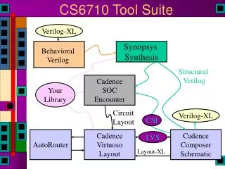
Cadence Design Phase Tips & Tricks: Maximizing Efficiency in EE Projects
110 likes | 174 Vues
Learn to estimate delay using stage effort, analyze area, create symbols from schematics, assemble blocks, and extract netlists effectively for efficient project design in Cadence. Avoid common pitfalls and pass LVS smoothly. Start early, check design frequently, and optimize layout productivity.

Cadence Design Phase Tips & Tricks: Maximizing Efficiency in EE Projects
E N D
Presentation Transcript
Project 2: Cadence Help Fall 2005 EE 141 Ke Lu
Design Phase • Estimate delay using stage effort. Example: 8 bit ripple adder driving a final load of 16. • Rough estimate of Area. Sum over the size times LE of every gate.
1. Transistor Level • Remember to use nmos4 and pmos4. • Make sure you have the right tech lib attached. 0.24u process. • Connect input and output pins accordingly.
2. Creating Symbol from Schematic • In Schematic view, click Design->Create Cell View->From Cell View. • Don’t bother making the symbol shape pretty because Cadence will crash.
3. Putting the Blocks Together • Use “i” to instantiate symbols to build more complicated schematics. • Use “l” hot key to label wire names to simplify connecting the blocks together. Example, VDD and GND.
Extracting Netlist • In Schematic view, open the analog environment window by clicking Tools-> Analog Environment. • Go to Setup-> Environment and change the settings to hSpice and hierarchal. • Next go to Setup-> Simulator/Directory/Host and change the Project Directory. • Finally, click Simulation-> Netlist-> Create Final • Cadence will put the netlist in CELLNAME/ hspiceS/extracted/netlist/hspiceFinal • Fix the model file by adding “.lib g25.mod TT”, change TSMC25DN to NMOS, and edit the .OPTION statement.
LAYOUT • Pitfalls • Doing LVS after laying out the entire adder. • Not running DRC often. • Not budgeting space for routing. • Plan ahead to avoid these. Otherwise, Cadence will make life miserable.
How to Pass LVS • Plan ahead before laying out. Do stick diagrams first. • Do LVS “incrementally.” • Example, mirror adder.
Summary • START EARLY. Cadence will hang as more and more people use the machines. • Check Design often, run DRC often. Catch bugs early. • Worst case tp*A = 6 uS * um^2. You must do better.
