CMOS Compatible Integrated Dielectric Optical Waveguide Coupler and Fabrication
120 likes | 364 Vues
2011-2 Special Topics in Optical Communications. CMOS Compatible Integrated Dielectric Optical Waveguide Coupler and Fabrication. Jeong -Min Lee ( minlj@tera.yonsei.ac.kr ) High-Speed Circuits and Systems LAB. 2011-2 Special Topics in Optical Communications. Information.

CMOS Compatible Integrated Dielectric Optical Waveguide Coupler and Fabrication
E N D
Presentation Transcript
2011-2 Special Topics in Optical Communications CMOS Compatible Integrated Dielectric Optical Waveguide Coupler and Fabrication Jeong-Min Lee (minlj@tera.yonsei.ac.kr) High-Speed Circuits and Systems LAB.
2011-2 Special Topics in Optical Communications Information • Name: CMOS Compatible Integrated Dielectric Optical Waveguide Coupler and Fabrication • United States Patent (Patent NO.: US 7,738,753 B2) • Date of Patent: Jun 15, 2010 • Inventors: Solomon Assefa • Assignee: IBM High-Speed Circuits and Systems LAB.
2011-2 Special Topics in Optical Communications Contents • Background of the Invention • Summary of the Invention • Fabrication Process (Detailed description) • Conclusion High-Speed Circuits and Systems LAB.
2011-2 Special Topics in Optical Communications Background of the Invention • Integrated semiconductor devices that include one or more photonic devices: Photodetectors, Modulators, and Optical switchesRequire a mechanism to couple optical signals between the optical fibers and the silicon based waveguides • Coupling from an optical fiber to a photonic device with input and output waveguides often suffers from loss due to index and mode-profile mismatches Polymer couplers • Technique used to minimize losses in coupling • Provide effective matching • Optoelectronic circuits (fabricating CMOS) Fabricating polymer couplers for use photonic devices need to be encapsulated and annealed as CMOS-compatible processes High-Speed Circuits and Systems LAB.
2011-2 Special Topics in Optical Communications Summary of Invention • This invention provides a method for encapsulation of the devices and the formation of the couplers Performance is not affected • This invention provides a CMOS compatible method: • Thermal treatment • Electrical activation • 3D integration of optical devices • This invention allows an efficiently manufactured semiconductor device that integrates photonic devices with CMOS circuit devices. High-Speed Circuits and Systems LAB.
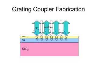
2011-2 Special Topics in Optical Communications Fabrication Process • Accept a semiconductor device with an Integrated Optoelectronic circuit and at least one waveguide (Fig. 1) • Depositing a lower SiN layer, an SiON layer, a DLC layer and an upper SiN layer (Fig. 1) High-Speed Circuits and Systems LAB.
2011-2 Special Topics in Optical Communications Fabrication Process • Deposit photo-resist layer with an etching area defining an optical wave guide coupler fabrication area (Fig. 1) • Etch a portion of the upper SiN layer under the etching area (Fig. 2) • DLC: CMP Stop Layer High-Speed Circuits and Systems LAB.
2011-2 Special Topics in Optical Communications Fabrication Process • Remove the photo-resist layer and a portion of the diamond like carbon(DLC) layer under the etching area (Fig. 3) • Etch the SiO2 layer to at least the lower SiNlayer (Fig. 4) High-Speed Circuits and Systems LAB.
2011-2 Special Topics in Optical Communications Fabrication Process • Depositing an SiON layer onto the semiconductor die (Fig. 5) • Perform CMP to remove the SiON layer not within the etching area and the upper SiNlayer (Fig. 6) • CMP: Chemical Mechanical Polishing High-Speed Circuits and Systems LAB.
2011-2 Special Topics in Optical Communications Fabrication Process • Etch the DLC layer to leave the SiO2 layer and SiON transition layer (Fig. 7) • Semiconductor die that has been cleaved along cleave line to expose an exposed face of the SiON coupler (Fig. 8) • An optical fiber is attached to the exposed face of the SiON coupler High-Speed Circuits and Systems LAB.
2011-2 Special Topics in Optical Communications Conclusion • This invention provides a method for encapsulation of the devices and the formation of the couplers • Polymer couplers • Low losses in coupling • Provide effective matching • photonic devices need to be encapsulated and annealed as CMOS-compatible processes High-Speed Circuits and Systems LAB.
2011-2 Special Topics in Optical Communications Thank you for listening Jeong-Min Lee (minlj@tera.yonsei.ac.kr) High-Speed Circuits and Systems