Download
1 / 57
590 likes | 918 Vues
Learn analog IC design techniques, amplifier types, layout considerations, CAD tools, grading breakdown, fabrication privilege, and ways to excel in the course.

E N D
EE 501 Analog IC Design • Instructor Contact Information • Name: Degang Chen • Office: 2134 Coover Hall • Email: djchen@iastate.edu • Phone: 294-6277 • Office Hour: MWF 12:00 – 2:00 pm Or any other time convenient to you • Please include "EE501" in the subject line in all email communications to avoid auto-deleting or junk-filtering
EE 501 Analog IC Design • TA Contact Information • Main TA: • Name: Tao Zeng • Office: 2135 Coover Hall • Phone: 515-708-3389 • Email: zt123@iastate.edu, • Helping TA: • Name: Jingbo Duan • Office: 2135 Coover Hall • Phone: 515-203-1784 • Email: duanjb@iastate.edu,
EE 501 Analog IC Design • Student Introduction • Contact information • For me to contact you • Brief intro • Name • Advisor • Area • Interest • IC design experience • Cadence experience • Study / lab partners
Class Webpage • http://class.ece.iastate.edu/djchen/ee501/2008 • Please check the page for • Any announcement • Class notes • HW assignments • Lab assignments • Project requirements • Class policy and other info
Student behavior expectations • Full attendance except with prior-notified excuses • On-time arrival • Active participation • Ask questions • Answer questions from instructor or students • Be cordial and considerate to other students and TA • Help each other • Promptly report/share problems/issues
Prohibited behaviors • Any foul language or gesture • Comments to other students that are discriminatory in any form • Any harassments as defined by the university • Academic dishonesty • No alcohol, drugs, or any other illegal / improper substances
Accommodation/Assistance • Please let me know if you • Have any special needs • Have disability in any form • Have any medical/mental/emergency conditions • Have field trips / interviews • Have special requests • Want me to adjust lecture contents/pace • Can also consult me if you • Would like to seek advice on any professional or personal issues • Would like to have certain confidential discussions
Course Description • Design techniques for analog and mixed-signal VLSI circuits. • Amplifiers: operational amplifiers, transconductance amplifiers, finite gain amplifiers and current amplifiers. • Linear building block: differential amplifiers, current mirrors, references, cascoding and buffering. • Performance characterization of linear integrated circuits: offset, noise, sensitivity and stability. • Layout considerations, simulation, yield and modeling for high-performance linear integrated circuits. • CAD tools: Cadence.
Final Grade Weighting • Laboratory: 25% • Design projects: 15% each • Homework: 15% • Midterm Exam: 10% • Final exam: 15% • Classroom participation: 5% • Bonus for original creative work (publishable/patentable work)
Fabrication Privilege • Circuit fabrication is not required for the course • It is offered free as a privilege • Requirements for this privilege • Detailed simulation results demonstrating that circuit is highly likely to work • Sufficient testing plan (what to measure and how) • Promise to test (availability and commitment of time) • Register in ee599CD and submit a report to MOSIS • Benefits: • Valuable experience • Increased marketability • Get one credit for fabrication and testing • Limits: max two submissions per student
Two Alternative Ways to Get A • Successful design of both projects • Both show A-level performance in schematic and post layout simulation, as well as well-thought-out layout • At least one project successfully fabricated and satisfactorily tested • Nontrivial originally contribution • Accepted technical paper to a decent conference and/or journal • Paper deemed at similar level by Instructor
Text Book • Allen and Holberg, CMOS Analog Circuit Design, 2nd Edition, Oxford, 2002 • Hastings, The Art of Analog Layout, Prentice Hall, 2nd ed • Available at Amazon • Significant discounts vs bookstore • Links in a previous email
References • Gray, et al, Analysis and Design of Analog Integrated Circuits, 4th Ed., Wiley, 2001 • William Liu, Mosfet Models for Spice Simulation, Including BSIM3v3 and BSIM4, Wiley-IEEE, 2001 • Daniel P. Foty, MOSFET Modeling With SPICE: Principles and Practice, Prentice Hall, 1996 • Yannis Tsividis, Operation and Modeling of the MOS Transistor, Oxford University Press; 2nd edition (May 1, 2003) • Laker and Sansen, Design of Analog Integrated Circuits, McGraw Hill, 1994 • David Johns & Ken Martin , Analog Integrated Circuit Design, John Wiley & Sons, Inc. 1997 • Behzad Razavi, Design of Analog CMOS Integrated, CircuitsMcGraw-Hill, 1999 • Geiger, et al, VLSI Design Techniques for Analog and Digital Circuit, McGraw Hill, 1990 • Baker, CMOS Circuit Design, Layout and Simulation, IEEE Press, 1997 • Alan B. Grebene, Bipolar and MOS Analog Integrated Circuit Design (Wiley Classics Library), 2001
VDD M1,2: 15/1.5 M3,4: 45/1.5 M5: 30/1.5 M0: 3/1.5 CL: 5 pF IB: 10 uA M3 M4 Vo CL IB M1 Vin- M2 Vin+ M5 M0 Lab 0
MOSIS links • MOSIS web site • FAQ from comp.lsi.cad • MOSIS scalable design rules • MOSIS Pads directory. • Process description: TSMC 0.25, AMI 0.5 • SPICE model parameters: TSMC 0.25, AMI 0.5
Links for information sources • IEEE IEL • Science Citation Index / ISI Web of Knowledge • U.S. Patent Office • International Technology Roadmap for Semiconductors • Semiconductor Research Corporation
Links for technical writing • Things to think about while writing papers • A nuts and bolts guide to college writing • The Barleby refence site • William Shrunk's "Elements of Style" • Dictionary.com • Visual Thesaurus • Latex style files for IEEE journals
“G source” “E source” “F source” “H source”
Closer View Of Polishing
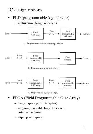
BASIC FABRTICATION PROCESSES • Oxide growth • Thermal diffusion • Ion implantation • Deposition • Etching • Photolithography
Oxidation • The process of growing a layer of silicon dioxide (SiO2)on the surface of a silicon wafer. • Uses: • Provide isolation between two layers • Protect underlying material from contamination • Very thin oxides (100 to 1000 Å) are grown using dry-oxidation techniques. • Thicker oxides (>1000 Å) are grown using wet oxidation techniques.
Diffusion Movement of impurity atoms at the surface of the silicon into the bulk of the silicon • From higher concentration to lower concentration. • Done at high temperatures: 800 to 1400 °C.
Ion Implantation The process by which impurity ions are accelerated to a high velocity and physically lodged into the target.
Require anneal to repair damage • Can implant through surface layers • Can achieve unique doping profile
Deposition • Chemical-vapor deposition (CVD) • Low-pressure chemical-vapor deposition • Plasma-assisted chemical-vapor deposition • Sputter deposition • Materials deposited • Silicon nitride (Si3N4) • Silicon dioxide (SiO2) • Aluminum • Polysilicon
Etching • To selectively remove a layer of material • But may remove portions or all of • The desired material • The underlying layer • The masking layer • Two basic types of etches: • Wet etch, uses chemicals • Dry etch, uses chemically active ionized gasses.