Understanding the 8086 Microprocessor Bus Cycle and Wait States
The 8086 microprocessor utilizes wait states to manage bus cycles, particularly when slower peripheral devices are present. When the READY input is set low, wait states are inserted between T3 and T4 of the bus cycle. This mechanism allows the processor to synchronize with external hardware demands. Various signals, including control, address, and data lines, play critical roles in bus operations. Our exploration covers pin definitions, operational modes of the 8086, and how these aspects can be enhanced to improve CPU performance aligning with modern microprocessor features.

Understanding the 8086 Microprocessor Bus Cycle and Wait States
E N D
Presentation Transcript
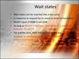
Wait states • Wait states can be inserted into a bus cycle • In response to request by an event in external hardware • READY input of 8086 is set LOW • As long as READY is held low, wait states (Tw) are inserted between T3 and T4 • For a write cycle, data maintained on the bus • Purpose: to extend the duration of the bus cycle, so slower memory devices can be used
Instruction sequence F8 50 B8 02 02
Pins definition • AD15 – AD0 Address/Data Bus • A19/S6 – A16/S3 - Address/Status • BHE/S7 – Bus high enable • MN/MX – min. max. mode control • RD – read control (read data from memory or I/O) • Test – wait on test (input). If test signal is HIGH then processor will be in an idle state • Ready – (input) wait state control • Reset – system reset (if kept HIGH for 4 clock cycles) • NMI – non-maskable interrupt request • INTR – interrrupt request • CLK – system clock
Pins definition • HOLD – hold request (used with DMA) • HLDA – hold acknowledge (entered the HOLD state) • WR – write control • M/IO – memory /IO control • DT/R – data transmit receive (to enable external data bus buffer) • DEN – data enable • ALE – address latch enable • INTA – interrupt acknowledge
Pins definition • RQ / GT1,0 – request / grant bus access control (Used in max. mode, to force the processor to release the local bus at the end of the processor’s current bus cycle) • LOCK – bus priority lock control (disable other bus master to gain access of the system bus) • /S2-/S0 – bus cycle status (this lines reflect the type of operation being carried out by the processor) • QS1 – QS0 – instruction queue status (give information about the status of the code-prefetch queue)
Instruction sequence 100 F8 50 B8 02 02 10
Status signals • S6 – S3 – are output on the bus at the same time that data are transferred over the other bus lines • S4 and S3 form a 2-bit binary code that identifies which of the 8086’s internal segment register was used to generate the physical address • 00 – extra 01 – stack 10 – code/none 11 – Data • S5 – logic level of the interrupt enable flag • S6 – not used always at 0
Control signals • Control signals are provided to support memory and I/O interfaces • ALE – 0-> 1 to signal external circuitry when a valid address word is on the bus • BHE : 0 used as memory enable for the most significant byte (High Byte) half of the data bus • M/IO: 1 represent a memory operation • 0 represent an I/O operation • DT/R: 1 bus in transmit mode; 0 in receive mode • RD: represent a read cycle and reading data from the bus • WR: represent a write cycle and 0 represent valid write or output data are on the bus • DEN: signals external devices when they should put data on the bus
Operating modes of 8086 • The 8086 can run in two different modes: minimum and maximum • In min. mode 8086 provides all the control signals needed to implement the memory I/O interfaces • In max. mode, it provides signals (status signals) for implementing a multiprocessor/coprocessor system environment • In max. mode, bus controller, bus arbiter are included in the system. The controller derives the control signals based on the status signals
Maximum mode • The basic functions of the bus controller chip (8288) is to derive control signals like /RD, /WR, /DEN, DT/R, ALE based on the status lines • /IORC, /IOWC – I/O read/write command signals. They enable an IO interface to read or write data from or to the addressed port. • /MRDC, /MWTC – memory read and write command signals. For instructing memory to accept or send data from or to the bus. • /AIOWC, /AMWTC – advanced /IOWC and /MWTC. Serve the same purpose as /IOWC or /MWTC but are activated one clock cycle earlier.
Minimum mode circuit Latch – store Transceiver – transmit + receive
Read cycle Why there are two address? Output From address latch Output from multiplexed Address/data bus
Memory To access the memory both address and data must be available at the same time. But for 8086, the bus is multiplexed so Physically it is not possible to supply both information simultaneously So address latches are used to hold the address information when the bus is used to transceive data memory Data Address
Modern microprocessor architecture Based on your understanding of the 8086 microprocessor, what features of the 8086 are needed to be modified in order to make it more powerful? What are the major differences between a modern microprocessor and a 8086???
Modern microprocessors • The following features are crucial to the performance: • Operating speed (clock rate) • Memory (size and speed) • Data size • Floating point processing • Overlapping of execution and memory access • Perform more tasks in a single cycle
Modern microprocessor • Operating speed • The 8086 operates at 5MHz • The latest Intel microprocessor (i5, i7, i9) can operate at the 2.6GHz range • The operating frequency is governed by the fabrication techniques (0.13 Micron technology for P4 and the 8086 is based on 3 Micron technology). With sub-micron technology we can put more components into the chip • The higher the operating speed, more heat will be generated and cooling the CPU becomes more important. No cooling is for the CPU is required in the 486 era
Modern microprocessor • Memory • The 8086 has 20-bit address bus and the max. memory location is only 1MBytes • The Pentium II can access up to 64GBytes (what is the size of the address bus???) of memory • The speed of memory chip has also increased in the last 20 years • The RDRAM can operate at 600MHz or 800MHz • What is the advantage(s) of having more memory??? • Using 8086 as an example, memory read/write must complete in 4 cycles so if the memory is slow then the memory read/write cannot be completed in 4 cycles.
Memory speed • To improve the performance, internal high-speed memory is provided for the storage of data as well as instruction. These internal memory is called cache • There are cache inside the CPU and it is called Level 1 (L1) cache (there are at least 8Kb in P4) • The cache located between the CPU and the external memory is called Level 2 (L2) cache (speed of cache is higher then the traditional memory) (512K in P4) • In newer microprocessors design, L2 cache is also located inside the CPU so therefore, L3 cache is also provided. L3 cache is external just like L2 cache in the old days.
Cache • Accessing data/instruction from cache is faster that accessing the traditional memory so when executing a program, if the entire program is already stored in the cache then the overall performance can be improved
Cache • Cache is fast • Access time for DRAM could be 60ns while for the cache it could be 15ns • to access cache memory the CPU does not have to use motherboard’s system bus (also slow) for data transfer.
CPU Memory L1 L2 Cache
Cache • The cache is usually divided into smaller units, called blocks. • In 486, the 8K cache is divided into 4 2K blocks. Each block is 16bytes x 128 rows • The 16-byte row is divided into 4-byte lines. Any of the 4 lines cannot be accessed partially. • During operations, the microprocessor always check the cache for data and instruction first. If data is already stored in the cache – it is called a cache hit • Usually a mechanism called paging is employed to write frequently used data and instruction into the cache • If the data is not found then – cache miss
Modern Microprocessor • Data • The 8086 has a 16-bit data bus • The P4 has a 64-bit data bus so can get more data in a single read/write cycle • Or processing of high-precision data can be more effective • Consider this: what is the maximum value can be represented by a 16-bit and a 32-bit pattern respectively
Overlapping of operations • In 8086 the instruction pipeline enables the overlapping of execution of instruction and fetching • In Pentium Pro processor which is a superscalar architecture – can execute multiple instructions concurrently • Two integer pipelines U and V, each one is 5-stage • One floating-point execution unit
Overlapping of operations • So it is possible to execute three instructions simultaneously (with proper programming the speedup can be up to 40%)
Pentium Processor • Pentium processor issues 2 instructions in parallel to the 2 independent integer pipelines (U and V) • This enhances the speed of integer arithmetic • In the prefetch stage, the CPU fetches instructions from the instruction cache • In Write Back, the CPU updates registers’ contents or the status in the flag register depending upon the execution result • In Pentium processor only one clock cycle to decode the instruction, comparing to 486, it takes 2 clock cycles.
Block diagram of Pentium processor Can you see the pipeline in the above?
Block diagram of U-V pipe for Pentium processor The pipeline of 8086 has how many stages?
The 8086 instruction execution sequence Fetch instruction Decode and determine operand address Fetch operand Execute Basic operations performed by a CPU
Modern microprocessor • Floating point hardware • Do you know how floating-point number is represented in a computer? • The floating-point hardware is an important design feature in modern processor • No floating-point hardware is available for 8086 • For Intel, the co-processor mechanism was used until the emerge of the 486 microprocessors
Perform more tasks in a single cycle • MMX – multimedia extension • It is for improving 2-D , 3-D multimedia applications • Using MMX instruction set, eight image elements (8-bit) can be loaded simultaneously and perform concurrent operation on them • The MMX instruction makes use of the 64-bit registers (the mantissa portion of the floating-point registers) • MMX instructions are mainly integer operations
MMX /SSE mechanism 128-bit register can Store 4 floating point value d1 d2 d3 d4 Operation d5 d6 d7 d8 result r1 r2 4 results can be obtained in one single operation r3 r4
Points about P4 • More features to support parallel processing – hyper-threading technology, SSE, MMX instructions, deeper pipeline, dual-core • Still compatible with existing Intel architecture based software • Operate at very high frequency up to 3GHz • With 8KB data cache and 12K instruction cache • Integer ALUs operate at twice the core processor frequency
Self-test • How to make a microprocessor to become more powerful! • What is the most important hardware feature embedded in a 8086 microprocessor? • What are the basic operations being performed when a computer is running? • What is the maximum value represented by a 20-bit pattern? • What is the maximum value represented by the sum of two 16-bit pattern? • What is the major function of a ALU? • What is the major functions of a BIU? • Can you use a block diagram to represent a memory? • What is an instruction pipeline and why it can improve the overall performance of a microprocessor?
Block diagram of Intel P4 CPU Can you spot any features come from the 8086 ?
Introduction to microcontroller • If you want to develop a simple robot are you going to use a P5 microprocessor in your system? • Usually to implement a simple system, microcontroller is used instead of a microprocessor. • A microcontroller can be regarded as an all-in-one device with a CPU, memory, Input/Output interfaces all included in a single package. Commonly used microcontrollers include the 8051 series, Basic Stamp, BasicX etc. In addition, the cost of a microcontroller is usually lower than the traditional microprocessor, for example an 8051 is only HKD25.
Some microcontrollers also come with additional features such as ADC (analog to digital converter), DAC (digital to analog converter) and PWM (pulse-width modulation) output. All those features are very useful for the implementation of basic robotic or control systems.
The ADuC832 device • The ADuC832 is a powerful microcontroller and is being used in the experimental setup. • Basic features of the device include: • 8-channel 12-bit ADC • 2 12-bit DAC • 62Kbytes Program memory, 4kBytes data memory • 2304 bytes on-chip data RAM • dual PWM output (the PWM can be used to control an analog device) • 8051 compatible instruction set • 4 8-bit Input/Output ports
Sensor ADuC832 Motor Motor Application using microcontroller • The components can be connected directly to the microcontroller via the I/O ports without other supporting devices.