Download
1 / 20
210 likes | 580 Vues
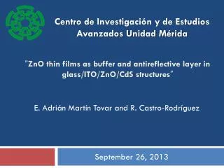
Centro de Investigación y de Estudios Avanzados Unidad Mérida. “ ZnO thin films as buffer and antireflective layer in glass/ITO/ZnO/ CdS structures ”. E. Adrián Martín Tovar and R. Castro-Rodríguez. September 26, 2013. Introduction.

E N D
Centro de Investigación y de Estudios Avanzados Unidad Mérida “ZnO thin films as buffer and antireflective layer in glass/ITO/ZnO/CdS structures” E. Adrián Martín Tovar and R. Castro-Rodríguez September 26, 2013
Introduction • Zinc Oxide (ZnO) is a II-VI semiconductor material withthefollowingproperties: • A 3.37 eV direct band gap • Thin film resistivity in therange of 10-4-1013 -cm • Refractiveindex of 2.03 • High transparency in the visible region of the electromagnetic spectrum • Crystallizes in three different phases : • Hexagonal wurtzite. • Zincblende • Rocksalt
Goals • Todeposit ZnO thin films using PLD techniquefortheir use as a buffer and anti-reflectivelayer in Glass/ITO/ZnO/CdSstructuresusingtwotypes of targets. For a buffer layerhighresistivities are required 102-103 -cm As an anti-reflectivelayer: Thickness of 80-150 nmforwavelenghts in a range of 650- 1200 nm
Experimental Procedures Vacuum of 10-5Torr What’s PLD? Laser pulse Nd:YAG =1064 nm ~2 J/(cm2) per shot 5 Hz Number of shots: 3000 Substrateheating Ts = 300° C Target-substratedistance 50 mm
Target (type A) • ZnO sinteredpowder, 99.99% • Area50.3 mm2 • Force = 10 Ton • T = 600° C (Heating) • Time = 2 hours
Target (Type B) • CuredpowderZnO, 99.99% • Mixedwithcyanoacrylate (C5H5NO2) • Proportion of 70:30 in weight (70% ZnO, 30% cyanoacrylate) • Dried at room temperature for three days
Thickness 80-150 nmforwavelenghts in a range of 650 a1200 nm
MorphologicalProperties Type A Type B
StructuralProperties • 36-1451 ICCD crystallographic letter associated with ZnO. • Hexagonal wurtzitestructure. • Preferential growth along the c-axis (002) • Displacements of diffraction peaks (002) to the left • FWHM (2) Type A
StructuralProperties • 36-1451 ICCD crystallographic letter associated with ZnO. • Preferential growth along (100) and (101) planes • Hexagonal wurtzitestructure. • Displacements of diffraction peaks (002) to the right • FWHM (2) Type B
StructuralesProperties • Nano-estructuredthin films • D fortype A suggests a quantum confinementeffect • A negative sign indicates that the unit cell of type A has a smaller volume than the standard unit cell • A positive sign indicates that the unit of type B has a greater volume than the standard unit cell Williamson Hall equation:
StructuralesProperties c c b b a a
OpticalProperties • Transmitance85% • Abortionedgeisn’tdefined UV VIS IR
PhotocurrentCalculations Elimination of 7.52% of losses Maximumvalue of 25.72 mA/cm2
ResitivityMeasures • Measuare at RT • ForCdS/CdTeSolar cells: 102 -103-cm
Conclusions • ZnO thin films were obtained through PLD by using two types targets. • Eg for the films A and B were 4.08 and 3.32 eV respectively • Egsample for type A is the result of quantum confinement effects.
Conclusions • The samples were suitable as anti-reflective coating, the presence of ZnO resulted in an increase of about 10% of transmittance in glass/ITO/ZnO/CdSstructures. • Photocurrent was obtained to be 19.04 and 19.09 mA/cm2 for samples A and B respectively, with a 7.52% elimination of photocurrent losses. • The type B film has the best results for an application as buffer layer and anti-reflective.